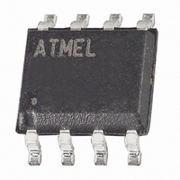
AT45DB021D-SH-T Atmel, AT45DB021D-SH-T Datasheet - Page 14

AT45DB021D-SH-T
Manufacturer Part Number
AT45DB021D-SH-T
Description
IC FLASH 2MBIT 66MHZ 8SOIC
Manufacturer
Atmel
Specifications of AT45DB021D-SH-T
Format - Memory
FLASH
Memory Type
DataFLASH
Memory Size
2M (1024 pages x 264 bytes)
Speed
66MHz
Interface
SPI, RapidS
Voltage - Supply
2.7 V ~ 3.6 V
Operating Temperature
-40°C ~ 85°C
Package / Case
8-SOIC (5.3mm Width), 8-SOP, 8-SOEIAJ
Cell Type
NOR
Density
2Mb
Access Time (max)
6ns
Interface Type
Serial (SPI)
Boot Type
Not Required
Address Bus
1b
Operating Supply Voltage (typ)
3/3.3V
Operating Temp Range
-40C to 85C
Package Type
SOIC EIAJ
Program/erase Volt (typ)
2.7 to 3.6V
Sync/async
Synchronous
Operating Temperature Classification
Industrial
Operating Supply Voltage (min)
2.7V
Operating Supply Voltage (max)
3.6V
Word Size
8b
Number Of Words
256K
Supply Current
15mA
Mounting
Surface Mount
Pin Count
8
Lead Free Status / RoHS Status
Lead free / RoHS Compliant
Available stocks
Company
Part Number
Manufacturer
Quantity
Price
Part Number:
AT45DB021D-SH-T
Manufacturer:
ATMEL/爱特梅尔
Quantity:
20 000
7.1.3
14
guaranteed. Furthermore, if more than 8-bytes of data is clocked into the device, then the data will wrap back
around to the beginning of the register. For instance, if 9-bytes of data are clocked in, then the ninth byte will be
stored at byte location zero of the Sector Protection Register.
If a value other than 00H or FFH is clocked into a byte location of the Sector Protection Register, then the
protection status of the sector corresponding to that byte location cannot be guaranteed. For example, if a value of
17H is clocked into byte location two of the Sector Protection Register, then the protection status of sector two
cannot be guaranteed.
The Sector Protection Register can be reprogrammed while the sector protection enabled or disabled. Being able
to reprogram the Sector Protection Register with the sector protection enabled allows the user to temporarily
disable the sector protection to an individual sector rather than disabling sector protection completely.
The Program Sector Protection Register command utilizes the internal SRAM buffer for processing. Therefore, the
contents of the buffer will be altered from its previous state when this command is issued.
Table 7-5.
Figure 7-3.
Read Sector Protection Register Command
To read the Sector Protection Register, the CS pin must first be asserted. Once the CS pin has been asserted, an
opcode of 32H and three dummy bytes must be clocked in via the SI pin. After the last bit of the opcode and
dummy bytes have been clocked in, any additional clock pulses on the SCK pins will result in data for the content
of the Sector Protection Register being output on the SO pin. The first byte corresponds to sector 0 (0a, 0b), the
second byte corresponds to sector one, the third byte corresponds to sector two, and the last byte (byte four)
corresponds to sector three. Once the last byte of the Sector Protection Register has been clocked out, any
additional clock pulses will result in undefined data being output on the SO pin. The CS must be deasserted to
terminate the Read Sector Protection Register operation and put the output into a high-impedance state.
Table 7-6.
Note:
Figure 7-4.
Command
Program Sector Protection Register
CS
Command
Read Sector Protection Register
CS
SO
Atmel AT45DB021D
SI
SI
xx = Dummy Byte
Each transition
represents 8 bits
Each transition
represents 8 bits
Program Sector Protection Register Command
Program Sector Protection Register
Read Sector Protection Register Command
Read Sector Protection Register
Opcode
Opcode
Byte 1
Opcode
X
Byte 2
X
Opcode
Byte 3
Byte 1
Byte 1
3DH
32H
X
Opcode
Byte 4
Data Byte
Byte 2
Byte 2
2AH
xxH
n
Data Byte
n
Data Byte
n + 1
Byte 3
Byte 3
Data Byte
7FH
xxH
n + 1
Data Byte
n + 3
Byte 4
Byte 4
FCH
xxH
Data Byte
n + 3
3638J–DFLASH–5/10


