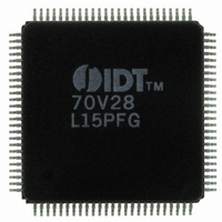
IDT70V28L15PFG IDT, Integrated Device Technology Inc, IDT70V28L15PFG Datasheet - Page 8

IDT70V28L15PFG
Manufacturer Part Number
IDT70V28L15PFG
Description
IC SRAM 1MBIT 15NS 100TQFP
Manufacturer
IDT, Integrated Device Technology Inc
Datasheet
1.IDT70V28L15PFG.pdf
(17 pages)
Specifications of IDT70V28L15PFG
Format - Memory
RAM
Memory Type
SRAM - Dual Port, Asynchronous
Memory Size
1M (64K x 16)
Speed
15ns
Interface
Parallel
Voltage - Supply
3 V ~ 3.6 V
Operating Temperature
0°C ~ 70°C
Package / Case
100-TQFP, 100-VQFP
Density
1Mb
Access Time (max)
15ns
Sync/async
Asynchronous
Architecture
Not Required
Clock Freq (max)
Not RequiredMHz
Operating Supply Voltage (typ)
3.3V
Address Bus
16b
Package Type
TQFP
Operating Temp Range
0C to 70C
Number Of Ports
2
Supply Current
235mA
Operating Supply Voltage (min)
3V
Operating Supply Voltage (max)
3.6V
Operating Temperature Classification
Commercial
Mounting
Surface Mount
Pin Count
100
Word Size
16b
Number Of Words
64K
Lead Free Status / RoHS Status
Lead free / RoHS Compliant
Other names
70V28L15PFG
800-1393
800-1393
Available stocks
Company
Part Number
Manufacturer
Quantity
Price
Company:
Part Number:
IDT70V28L15PFG
Manufacturer:
IDT, Integrated Device Technology Inc
Quantity:
10 000
Company:
Part Number:
IDT70V28L15PFG8
Manufacturer:
IDT, Integrated Device Technology Inc
Quantity:
10 000
Company:
Part Number:
IDT70V28L15PFGI
Manufacturer:
THOMBETT
Quantity:
3 072
Timing Waveform of Write Cycle No. 1, R/W Controlled Timing
Timing Waveform of Write Cycle No. 2, CE Controlled Timing
CE or SEM
ADDRESS
CE or SEM
NOTES:
1. R/W or CE or UB and LB = V
2. A write occurs during the overlap (t
3. t
4. During this period, the I/O pins are in the output state and input signals must not be applied.
5. If the CE or SEM = V
6. Timing depends on which enable signal is asserted last, CE or R/W.
7. This parameter is guaranteed by device characterization, but is not production tested. Transition is measured 0mV from steady state with the Output Test Load
8. If OE = V
9. To access RAM, CE = V
10. Refer to Truth Table I - Chip Enable.
ADDRESS
DATA
UB or LB
IDT70V28L
High-Speed 3.3V 64K x 16 Dual-Port Static RAM
UB or LB
DATA
(Figure 2).
placed on the bus for the required t
specified t
DATA
WR
is measured from the earlier of CE or R/W (or SEM or R/W) going HIGH to the end of write cycle.
R/W
R/W
OUT
OE
IN
IN
(9)
WP
(9,10)
(9,10)
(9)
IL
.
during R/W controlled write cycle, the write pulse width must be the larger of t
IL
transition occurs simultaneously with or after the R/W = V
IL
and SEM = V
IH
during all address transitions.
t
EW
AS
DW
t
AS
(6)
or t
. If OE = V
IH
(6)
WP
. To access semaphore, CE = V
) of a CE = V
(4)
IH
during an R/W controlled write cycle, this requirement does not apply and the write pulse can be as short as the
IL
t
and a R/W = V
WZ
(7)
t
t
AW
AW
t
WC
t
WC
t
t
EW
WP
IH
IL
and SEM = V
for memory array writing cycle.
(2)
(2)
IL
8
transition, the outputs remain in the High-impedance state.
IL
. t
t
t
DW
DW
EW
must be met for either condition.
WP
or (t
t
WZ
WR
Industrial and Commercial Temperature Ranges
+ t
(3)
DW
t
t
DH
t
DH
) to allow the I/O drivers to turn off and data to be
WR
t
OW
(3)
t
HZ
(7)
(4)
(1,5)
(1,5,8)
4849 drw 08
4849 drw 07
.


