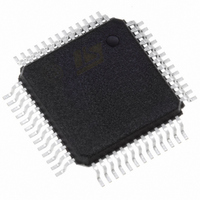
PSD834F2V-15M STMicroelectronics, PSD834F2V-15M Datasheet - Page 37

PSD834F2V-15M
Manufacturer Part Number
PSD834F2V-15M
Description
IC FLASH 2MBIT 150NS 52QFP
Manufacturer
STMicroelectronics
Datasheet
1.PSD813F2VA-20JI.pdf
(109 pages)
Specifications of PSD834F2V-15M
Format - Memory
FLASH
Memory Type
FLASH
Memory Size
2M (256K x 8)
Speed
150ns
Interface
Parallel
Voltage - Supply
3 V ~ 3.6 V
Operating Temperature
0°C ~ 70°C
Package / Case
52-QFP
Lead Free Status / RoHS Status
Lead free / RoHS Compliant
Other names
497-2011
Available stocks
Company
Part Number
Manufacturer
Quantity
Price
Company:
Part Number:
PSD834F2V-15M
Manufacturer:
STMicroelectronics
Quantity:
10 000
Output Macrocell (OMC)
Eight of the Output Macrocells (OMC) are con-
nected to Ports A and B pins and are named as
McellAB0-McellAB7. The other eight macrocells
are connected to Ports B and C pins and are
named as McellBC0-McellBC7. If an McellAB out-
put is not assigned to a specific pin in PSDabel,
the Macrocell Allocator block assigns it to either
Port A or B. The same is true for a McellBC output
on Port B or C. Table
port assignment.
The Output Macrocell (OMC) architecture is
shown in
ure, there are native product terms available from
the AND Array, and borrowed product terms avail-
able (if unused) from other Output Macrocells
(OMC). The polarity of the product term is con-
Table 15. Output Macrocell Port and Data Bit Assignments
Macrocell
McellAB0
McellAB1
McellAB2
McellAB3
McellAB4
McellAB5
McellAB6
McellAB7
McellBC0
McellBC1
McellBC2
McellBC3
McellBC4
McellBC5
McellBC6
McellBC7
Output
Figure 16., page
Assignment
Port B0, C0
Port B1, C1
Port B2, C2
Port B3, C3
Port B4, C4
Port B5, C5
Port B6, C6
Port B7, C7
Port A0, B0
Port A1, B1
Port A2, B2
Port A3, B3
Port A4, B4
Port A5, B5
Port A6, B6
Port A7, B7
15
Port
shows the macrocells and
39. As shown in the fig-
Native Product Terms
Doc ID 10552 Rev 3
3
3
3
3
3
3
3
3
4
4
4
4
4
4
4
4
trolled by the XOR gate. The Output Macrocell
(OMC) can implement either sequential logic, us-
ing the flip-flop element, or combinatorial logic.
The multiplexer selects between the sequential or
combinatorial logic outputs. The multiplexer output
can drive a port pin and has a feedback path to the
AND Array inputs.
The flip-flop in the Output Macrocell (OMC) block
can be configured as a D, T, JK, or SR type in the
PSDabel program. The flip-flop’s clock, preset,
and clear inputs may be driven from a product
term of the AND Array. Alternatively, CLKIN (PD1)
can be used for the clock input to the flip-flop. The
flip-flop is clocked on the rising edge of CLKIN
(PD1). The preset and clear are active High inputs.
Each clear input can use up to two product terms.
Maximum Borrowed
Product Terms
6
6
6
6
6
6
6
6
5
5
5
5
6
6
6
6
PSD813F2V, PSD854F2V
Data Bit for Loading or
Reading
D0
D1
D2
D3
D4
D5
D6
D7
D0
D1
D2
D3
D4
D5
D6
D7
37/109


