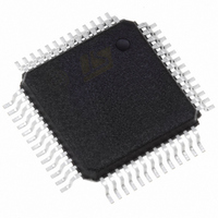
PSD834F2V-15M STMicroelectronics, PSD834F2V-15M Datasheet - Page 28

PSD834F2V-15M
Manufacturer Part Number
PSD834F2V-15M
Description
IC FLASH 2MBIT 150NS 52QFP
Manufacturer
STMicroelectronics
Datasheet
1.PSD813F2VA-20JI.pdf
(109 pages)
Specifications of PSD834F2V-15M
Format - Memory
FLASH
Memory Type
FLASH
Memory Size
2M (256K x 8)
Speed
150ns
Interface
Parallel
Voltage - Supply
3 V ~ 3.6 V
Operating Temperature
0°C ~ 70°C
Package / Case
52-QFP
Lead Free Status / RoHS Status
Lead free / RoHS Compliant
Other names
497-2011
Available stocks
Company
Part Number
Manufacturer
Quantity
Price
Company:
Part Number:
PSD834F2V-15M
Manufacturer:
STMicroelectronics
Quantity:
10 000
PSD813F2V, PSD854F2V
SPECIFIC FEATURES
Flash Memory Sector Protect
Each primary and secondary Flash memory sector
can be separately protected against Program and
Erase cycles. Sector Protection provides addition-
al data security because it disables all Program or
Erase cycles. This mode can be activated through
the JTAG Port or a Device Programmer.
Sector protection can be selected for each sector
using the PSDsoft Express Configuration pro-
gram. This automatically protects selected sectors
when the device is programmed through the JTAG
Port or a Device Programmer. Flash memory sec-
tors can be unprotected to allow updating of their
contents using the JTAG Port or a Device Pro-
grammer. The MCU can read (but cannot change)
the sector protection bits.
Any attempt to program or erase a protected Flash
memory sector is ignored by the device. The Verify
operation results in a READ of the protected data.
This allows a guarantee of the retention of the Pro-
tection status.
The sector protection status can be read by the
MCU through the Flash memory protection and
PSD/EE protection registers (in the CSIOP block).
See Tables
Reset Flash
The Reset Flash instruction consists of one
WRITE cycle (see
be optionally preceded by the standard two
WRITE decoding cycles (writing AAh to 555h and
55h to AAAh). It must be executed after:
–
–
Table 11. Sector Protection/Security Bit Definition – Flash Protection Register
Note: 1. Bit Definitions:
Table 12. Sector Protection/Security Bit Definition – PSD/EE Protection Register
Note: 1. Bit Definitions:
28/109
Bit 7
Sec7_Prot
Bit 7
Security_Bit
Reading the Flash Protection Status or Flash
ID
An Error condition has occurred (and the
device has set the Error Flag Bit (DQ5) to '1')
during a Flash memory Program or Erase
cycle.
Sec<i>_Prot 1 = Primary Flash memory or secondary Flash memory Sector <i> is write protected.
Sec<i>_Prot 0 = Primary Flash memory or secondary Flash memory Sector <i> is not write protected.
Sec<i>_Prot 1 = Secondary Flash memory Sector <i> is write protected.
Sec<i>_Prot 0 = Secondary Flash memory Sector <i> is not write protected.
Security_Bit 0 = Security Bit in device has not been set.
1 = Security Bit in device has been set.
11
Bit 6
Sec6_Prot
Bit 6
not used
and 12.
Table 9., page
Bit 5
Bit 5
Sec5_Prot
not used
21). It can also
Bit 4
Sec4_Prot
Bit 4
not used
Doc ID 10552 Rev 3
Bit 3
Bit 3
Sec3_Prot
Sec3_Prot
On the PSD813F2/3/4/5, the Reset Flash instruc-
tion puts the Flash memory back into normal
READ Mode. It may take the Flash memory up to
a few milliseconds to complete the Reset cycle.
The Reset Flash instruction is ignored when it is is-
sued during a Program or Bulk Erase cycle of the
Flash memory. The Reset Flash instruction aborts
any on-going Sector Erase cycle, and returns the
Flash memory to the normal READ Mode within a
few milliseconds.
On the PSD83xF2 or PSD85xF2, the Reset Flash
instruction puts the Flash memory back into nor-
mal READ Mode. If an Error condition has oc-
curred (and the device has set the Error Flag Bit
(DQ5) to '1') the Flash memory is put back into nor-
mal READ Mode within 25μs of the Reset Flash in-
struction having been issued. The Reset Flash
instruction is ignored when it is issued during a
Program or Bulk Erase cycle of the Flash memory.
The Reset Flash instruction aborts any on-going
Sector Erase cycle, and returns the Flash memory
to the normal READ Mode within 25μs.
Reset (RESET) Signal (on the PSD83xF2 and
PSD85xF2)
A pulse on Reset (RESET) aborts any cycle that is
in progress, and resets the Flash memory to the
READ Mode. When the reset occurs during a Pro-
gram or Erase cycle, the Flash memory takes up
to 25μs to return to the READ Mode. It is recom-
mended that the Reset (RESET) pulse (except for
Power On Reset, as described on
AND DEVICE STATUS AT RESET, page
at least 25μs so that the Flash memory is always
ready for the MCU to fetch the bootstrap instruc-
tions after the Reset cycle is complete.
Bit 2
Sec2_Prot
Bit 2
Sec2_Prot
Bit 1
Sec1_Prot
Bit 1
Sec1_Prot
RESET TIMING
Bit 0
Sec0_Prot
Bit 0
Sec0_Prot
67) be


