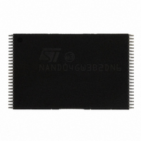
NAND04GW3B2DN6E NUMONYX, NAND04GW3B2DN6E Datasheet - Page 7

NAND04GW3B2DN6E
Manufacturer Part Number
NAND04GW3B2DN6E
Description
IC FLASH 4GBIT 48TSOP
Manufacturer
NUMONYX
Datasheet
1.NAND04GW3B2DN6E.pdf
(72 pages)
Specifications of NAND04GW3B2DN6E
Format - Memory
FLASH
Memory Type
FLASH - Nand
Memory Size
4G (512M x 8)
Interface
Parallel
Voltage - Supply
2.7 V ~ 3.6 V
Operating Temperature
-40°C ~ 85°C
Package / Case
48-TSOP
Lead Free Status / RoHS Status
Lead free / RoHS Compliant
Speed
-
Lead Free Status / RoHS Status
Lead free / RoHS Compliant
Available stocks
Company
Part Number
Manufacturer
Quantity
Price
Company:
Part Number:
NAND04GW3B2DN6E
Manufacturer:
StarMicro
Quantity:
872
Company:
Part Number:
NAND04GW3B2DN6E
Manufacturer:
ST
Quantity:
5 645
Part Number:
NAND04GW3B2DN6E
Manufacturer:
ST
Quantity:
20 000
NAND04G-B2D, NAND08G-BxC
1
Description
The NAND04G-B2D and NAND08G-BxC are part of the NAND flash 2112-byte/1056-word
page family of non-volatile flash memories. They use NAND cell technology have a density
of 4 Gbits and 8 Gbits, respectively.
The NAND04G-B2D memory array is split into 2 planes of 2048 blocks each. This
multiplane architecture makes it possible to program 2 pages at a time (one in each plane),
or to erase 2 blocks at a time (one in each plane). This feature reduces the average program
and erase times by 50%.
The NAND08G-BxC is a stacked device that combines two NAND04G-B2D dice, both of
which feature a multiplane architecture.
In the NAND08G-B2C devices, only one of the memory components can be enabled at a
time, therefore, operations can only be performed on one of the memory components at any
one time.
The devices operate from a 1.8 V or 3 V voltage supply. Depending on whether the device
has a x8 or x16 bus width, the page size is 2112 bytes (2048 + 64 spare) or 1056 words
(1024 + 32 spare), respectively.
The address lines are multiplexed with the data input/output signals on a multiplexed x8
input/output bus. This interface reduces the pin count and makes it possible to migrate to
other densities without changing the footprint.
Each block can be programmed and erased up to 100,000 cycles with ECC (error correction
code) on. To extend the lifetime of NAND flash devices, the implementation of an ECC is
mandatory.
A write protect pin is available to provide hardware protection against program and erase
operations.
The devices feature an open-drain ready/busy output that identifies if the P/E/R
(program/erase/read) controller is currently active. The use of an open-drain output allows
the ready/busy pins from several memories to connect to a single pull-up resistor.
A Copy Back Program command is available to optimize the management of defective
blocks. When a page program operation fails, the data can be programmed in another page
without having to resend the data to be programmed. An embedded error detection code
(EDC) is automatically executed after each copy back operation: 1 error bit can be detected
for every 528 bytes. With this feature it is no longer necessary to use an external ECC to
detect copy back operation errors.
The devices have a cache read feature that improves the read throughput for large files.
During cache reading, the device loads the data in a cache register while the previous data
is transferred to the I/O buffers to be read.
The devices have the chip enable ‘don’t care’ feature, which allows code to be directly
downloaded by a microcontroller. This is possible because chip enable transitions during the
latency time do not stop the read operation.
Both the NAND04G-B2D and NAND08G-BxC support the ONFI 1.0 specification.
The devices are available in the following packages:
TSOP48 (12 x 20 mm)
ULGA52 (12 x 17 x 0.65 mm)
Description
7/72


