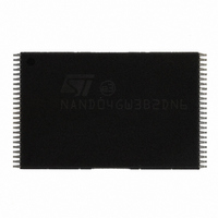
NAND04GW3B2DN6E NUMONYX, NAND04GW3B2DN6E Datasheet - Page 38

NAND04GW3B2DN6E
Manufacturer Part Number
NAND04GW3B2DN6E
Description
IC FLASH 4GBIT 48TSOP
Manufacturer
NUMONYX
Datasheet
1.NAND04GW3B2DN6E.pdf
(72 pages)
Specifications of NAND04GW3B2DN6E
Format - Memory
FLASH
Memory Type
FLASH - Nand
Memory Size
4G (512M x 8)
Interface
Parallel
Voltage - Supply
2.7 V ~ 3.6 V
Operating Temperature
-40°C ~ 85°C
Package / Case
48-TSOP
Lead Free Status / RoHS Status
Lead free / RoHS Compliant
Speed
-
Lead Free Status / RoHS Status
Lead free / RoHS Compliant
Available stocks
Company
Part Number
Manufacturer
Quantity
Price
Company:
Part Number:
NAND04GW3B2DN6E
Manufacturer:
StarMicro
Quantity:
872
Company:
Part Number:
NAND04GW3B2DN6E
Manufacturer:
ST
Quantity:
5 645
Part Number:
NAND04GW3B2DN6E
Manufacturer:
ST
Quantity:
20 000
Device operations
6.12
6.13
38/72
Read status enhanced
In NAND flash devices with multiplane architecture, it is possible to independently read the
status register of a single plane using the Read Status Enhanced command. If the error bit
of the status register, SR0, reports an error during or after a multiplane operation, the Read
Status Enhanced command is used to know which of the two planes contains the page that
failed the operation. Three address cycles are required to address the selected block and
page (A12-A28 for x8 devices and A11-A27 for x16 devices).
The output of the Read Status Enhanced command has the same coding as the Read
Status command. See
enhanced waveform.
Read EDC status register
The devices contain an EDC status register, which provides information on the errors that
occurred during the read cycles of the copy back and multiplane copy back operations. In
the case of multiplane copy back program, it is not possible to distinguish which of the two
read operations caused the error.
The EDCS status register is read by issuing the Read EDC Status Register command.
After issuing the Read EDC Status Register command, a read cycle outputs the content of
the EDC status register to the I/O pins on the falling edge of Chip Enable or Read Enable
signals, whichever occurs last. The operation is similar to Read Status Register command.
Table 15: EDC status register bits
for a description of Read EDC Status Register waveforms.
Table 15.
1. See
Bit
0
1
2
3
4
5
6
7
Table 14: Status register bits
EDC status register bits
Ready/busy
Ready/busy
Write protect
EDC validity
EDC status
Reserved
Reserved
Pass/fail
Table 14
Name
for a description of SR5 and SR6 bits.
(1)
(1)
for a full description and
summarizes the EDC status register bits. See
Logic level
‘don’t care’
‘don’t care’
‘1’
‘0’
‘1’
‘0’
‘1’
‘0’
‘1’
‘0’
‘1’
‘0’
‘1’
‘0’
Copy back or multiplane copy back
operation failed
Copy back or multiplane copy back
operation succeeded
Error
No error
Valid
Invalid
–
–
Ready
Busy
Ready
Busy
Not protected
Protected
Figure 30
NAND04G-B2D, NAND08G-BxC
Definition
for the read status
Figure 29


