CY7C1399BN-12VXC Cypress Semiconductor Corp, CY7C1399BN-12VXC Datasheet - Page 3
CY7C1399BN-12VXC
Manufacturer Part Number
CY7C1399BN-12VXC
Description
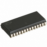
IC SRAM 256KBIT 12NS 28SOJ
Manufacturer
Cypress Semiconductor Corp
Type
Asynchronousr
Datasheet
1.CY7C1399BN-12ZXC.pdf
(8 pages)
Specifications of CY7C1399BN-12VXC
Memory Size
256K (32K x 8)
Package / Case
28-SOJ
Format - Memory
RAM
Memory Type
SRAM - Asynchronous
Speed
12ns
Interface
Parallel
Voltage - Supply
3 V ~ 3.6 V
Operating Temperature
0°C ~ 70°C
Access Time
12 ns
Supply Voltage (max)
3.6 V
Supply Voltage (min)
3 V
Maximum Operating Current
55 mA
Maximum Operating Temperature
+ 70 C
Minimum Operating Temperature
0 C
Mounting Style
SMD/SMT
Number Of Ports
1
Operating Supply Voltage
3.3 V
Density
256Kb
Access Time (max)
12ns
Sync/async
Asynchronous
Architecture
Not Required
Clock Freq (max)
Not RequiredMHz
Operating Supply Voltage (typ)
3.3V
Address Bus
15b
Package Type
SOJ
Operating Temp Range
0C to 70C
Supply Current
55mA
Operating Supply Voltage (min)
3V
Operating Supply Voltage (max)
3.6V
Operating Temperature Classification
Commercial
Mounting
Surface Mount
Pin Count
28
Word Size
8b
Number Of Words
32K
Memory Configuration
32K X 8
Supply Voltage Range
3V To 3.6V
Memory Case Style
SOJ
No. Of Pins
28
Operating Temperature Range
0°C To +70°C
Rohs Compliant
Yes
Lead Free Status / RoHS Status
Lead free / RoHS Compliant
Lead Free Status / RoHS Status
Lead free / RoHS Compliant, Lead free / RoHS Compliant
Other names
428-1988-5
CY7C1399BN-12VXC
CY7C1399BN-12VXC
Available stocks
Company
Part Number
Manufacturer
Quantity
Price

Part Number:
CY7C1399BN-12VXC
Manufacturer:
CYPRESS/赛普拉斯
Quantity:
20 000


Document #: 001-06490 Rev. *C
Capacitance
AC Test Loads and Waveforms
Switching Characteristics
Read Cycle
t
t
t
t
t
t
t
t
t
t
t
Write Cycle
t
t
t
t
t
t
t
t
t
t
Notes:
C
C
C
RC
AA
OHA
ACE
DOE
LZOE
HZOE
LZCE
HZCE
PU
PD
WC
SCE
AW
HA
SA
PWE
SD
HD
HZWE
LZWE
4. Tested initially and after any design or process changes that may affect these parameters.
5. Test conditions assume signal transition time of 3 ns or less, timing reference levels of 1.5V, input pulse levels of 0 to 3.0V, and output loading of the specified
6. At any given temperature and voltage condition, t
7. t
8. The internal write time of the memory is defined by the overlap of CE LOW and WE LOW. Both signals must be LOW to initiate a write and either signal can
9. The minimum write cycle time for write cycle #3 (WE controlled, OE LOW) is the sum of t
Parameter
OUTPUT
IN
IN
OUT
INCLUDING
I
terminate a write by going HIGH. The data input set-up and hold timing should be referenced to the rising edge of the signal that terminates the write.
JIG AND
OL
HZOE
: Addresses
: Controls
SCOPE
3.3V
/I
OH
, t
and capacitance C
HZCE
Parameter
[8, 9]
, t
C
HZWE
L
[4]
Read Cycle Time
Address to Data Valid
Data Hold from Address Change
CE LOW to Data Valid
OE LOW to Data Valid
OE LOW to Low Z
OE HIGH to High Z
CE LOW to Low Z
CE HIGH to High Z
CE LOW to Power-Up
CE HIGH to Power-Down
Write Cycle Time
CE LOW to Write End
Address Set-Up to Write End
Address Hold from Write End
Address Set-Up to Write Start
WE Pulse Width
Data Set-Up to Write End
Data Hold from Write End
WE LOW to High Z
WE HIGH to Low Z
are specified with C
R1 317
L
= 30 pF.
R2
351
Description
[6]
Over the Operating Range
[6]
L
[6, 7]
[8]
[6]
[6, 7]
Input Capacitance
Output Capacitance
GND
= 5 pF as in AC Test Loads. Transition is measured ±500 mV from steady state voltage.
3.0V
3 ns
[5]
Description
HZCE
10%
is less than t
ALL INPUT PULSES
90%
LZCE
Min.
12
12
3
0
3
0
8
8
0
0
8
7
0
3
, t
HZOE
[5]
T
V
A
CC
-12
= 25C, f = 1 MHz,
is less than t
= 3.3V
Max.
Test Conditions
12
12
12
5
5
6
7
90%
HZWE
10%
LZOE
3 ns
and t
, and t
Min.
15
15
10
10
10
SD
3
0
3
0
0
0
8
0
3
.
HZWE
-15
Equivalent to:
is less than t
Max.
OUTPUT
15
15
15
6
6
7
7
LZWE
Max.
5
6
6
THÉVENIN EQUIVALENT
for any given device.
CY7C1399BN
167
Unit
ns
ns
ns
ns
ns
ns
ns
ns
ns
ns
ns
ns
ns
ns
ns
ns
ns
ns
ns
ns
ns
Page 3 of 8
Unit
pF
pF
pF
1.73V
[+] Feedback
Related parts for CY7C1399BN-12VXC
Image
Part Number
Description
Manufacturer
Datasheet
Request
R

Part Number:
Description:
IC SRAM 256KBIT 15NS 28TSOP
Manufacturer:
Cypress Semiconductor Corp
Datasheet:

Part Number:
Description:
IC SRAM 256KBIT 12NS 28SOJ
Manufacturer:
Cypress Semiconductor Corp
Datasheet:
Part Number:
Description:
CY7C1399BN-12VXCT
Manufacturer:
Cypress Semiconductor Corp
Datasheet:
Part Number:
Description:
CY7C1399BN-12VXIT
Manufacturer:
Cypress Semiconductor Corp
Datasheet:
Part Number:
Description:
CY7C1399BN-12ZXCT
Manufacturer:
Cypress Semiconductor Corp
Datasheet:
Part Number:
Description:
CY7C1399BN-15VXA
Manufacturer:
Cypress Semiconductor Corp
Datasheet:
Part Number:
Description:
CY7C1399BN-15VXAT
Manufacturer:
Cypress Semiconductor Corp
Datasheet:
Part Number:
Description:
CY7C1399BN-15ZXIT
Manufacturer:
Cypress Semiconductor Corp
Datasheet:
Part Number:
Description:
IC SRAM 256KBIT 12NS 28TSOP
Manufacturer:
Cypress Semiconductor Corp
Datasheet:
Part Number:
Description:
IC SRAM 256KBIT 15NS 28SOJ
Manufacturer:
Cypress Semiconductor Corp
Datasheet:
Part Number:
Description:
IC SRAM 256KBIT 15NS 28SOJ
Manufacturer:
Cypress Semiconductor Corp
Datasheet:
Part Number:
Description:
IC SRAM 256KBIT 15NS 28SOJ
Manufacturer:
Cypress Semiconductor Corp
Datasheet:
Part Number:
Description:
IC SRAM 256KBIT 15NS 28SOJ
Manufacturer:
Cypress Semiconductor Corp
Datasheet:
Part Number:
Description:
IC SRAM 256KBIT 15NS 28TSOP
Manufacturer:
Cypress Semiconductor Corp
Datasheet:
Part Number:
Description:
IC SRAM 256KBIT 15NS 28TSOP
Manufacturer:
Cypress Semiconductor Corp
Datasheet: