CY7C1399BN-15ZXI Cypress Semiconductor Corp, CY7C1399BN-15ZXI Datasheet
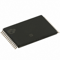
IC SRAM 256KBIT 15NS 28TSOP

CY7C1399BN-15ZXI

Manufacturer Part Number
CY7C1399BN-15ZXI
Description
IC SRAM 256KBIT 15NS 28TSOP
Manufacturer
Cypress Semiconductor Corp
Type
Asynchronousr
Datasheet

Specifications of CY7C1399BN-15ZXI

Memory Size
256K (32K x 8)
Package / Case
28-TSOP I
Format - Memory
RAM
Memory Type
SRAM - Asynchronous
Speed
15ns
Interface
Parallel
Voltage - Supply
3 V ~ 3.6 V
Operating Temperature
-40°C ~ 85°C
Access Time
15 ns
Supply Voltage (max)
3.6 V
Supply Voltage (min)
3 V
Maximum Operating Current
50 mA
Maximum Operating Temperature
+ 85 C
Minimum Operating Temperature
- 40 C
Mounting Style
SMD/SMT
Number Of Ports
1
Operating Supply Voltage
3.3 V
Lead Free Status / RoHS Status
Lead free / RoHS Compliant
Lead Free Status / RoHS Status
Lead free / RoHS Compliant, Lead free / RoHS Compliant
Other names
428-1991
CY7C1399BN-15ZXI

Available stocks

Company
Part Number
Manufacturer
Quantity
Price
Part Number:
CY7C1399BN-15ZXI
Manufacturer:
CYPRESS
Quantity:
717
Features
Functional Description
The CY7C1399BN is a high-performance 3.3V CMOS Static
RAM organized as 32,768 words by 8 bits. Easy memory
Selection Guide
Note:
Cypress Semiconductor Corporation
Document #: 001-06490 Rev. *C
1. For guidelines on SRAM system design, please refer to the ‘System Design Guidelines’ Cypress application note, available on the internet at www.cypress.com.
• Temperature Ranges
• Single 3.3V power supply
• Ideal for low-voltage cache memory applications
• High speed: 12 ns
• Low active power
• Low-power alpha immune 6T cell
• Available in Pb-free and non Pb-free Plastic SOJ and
Maximum Access Time (ns)
Maximum Operating Current (mA)
Maximum CMOS Standby Current (A)
Logic Block Diagram
— Industrial: –40°C to 85°C
— Automotive-A: –40°C to 85°C
— 180 mW (max.)
TSOP I packages
CE
WE
OE
A
A
A
A
A
A
A
A
A
A
0
1
2
3
4
5
6
7
8
9
[1]
INPUT BUFFER
DECODER
32K x 8
ARRAY
COLUMN
198 Champion Court
Commercial
Commercial (L)
Industrial
Automotive-A
POWER
DOWN
expansion is provided by an active LOW Chip Enable (CE) and
active LOW Output Enable (OE) and tristate drivers. The
device has an automatic power-down feature, reducing the
power consumption by more than 95% when deselected.
An active LOW Write Enable signal (WE) controls the
writing/reading operation of the memory. When CE and WE
inputs are both LOW, data on the eight data input/output pins
(I/O
addressed by the address present on the address pins (A
through A
the device and enabling the outputs, CE and OE active LOW,
while WE remains inactive or HIGH. Under these conditions,
the contents of the location addressed by the information on
address pins is present on the eight data input/output pins.
The input/output pins remain in a high-impedance state unless
the chip is selected, outputs are enabled, and Write Enable
(WE) is HIGH. The CY7C1399BN is available in 28-pin
standard 300-mil-wide SOJ and TSOP Type I packages.
0
through I/O
256K (32K x 8) Static RAM
14
San Jose
). Reading the device is accomplished by selecting
I/O
I/O
I/O
I/O
I/O
I/O
I/O
I/O
7
0
1
2
3
4
5
6
7
) is written into the memory location
500
500
-12
,
12
55
50
CA 95134-1709
Pin Configurations
GND
I/O
I/O
I/O
A
A
A
A
A
Revised October 8, 2010
A
A
A
A
A
10
11
12
13
14
5
6
7
8
9
0
1
2
13
14
1
2
3
4
5
6
7
8
9
10
11
12
CY7C1399BN
Top View
SOJ
28
27
26
25
24
23
22
21
20
19
18
17
16
15
500
500
-15
15
50
408-943-2600
I/O
V
WE
A
A
A
A
OE
A
CE
I/O
I/O
I/O
I/O
CC
4
3
2
1
0
3
7
6
5
4
0
[+] Feedback

Related parts for CY7C1399BN-15ZXI

CY7C1399BN-15ZXI Summary of contents

Page 1

... The input/output pins remain in a high-impedance state unless the chip is selected, outputs are enabled, and Write Enable (WE) is HIGH. The CY7C1399BN is available in 28-pin standard 300-mil-wide SOJ and TSOP Type I packages. INPUT BUFFER 32K x 8 ...

Page 2

... Max mA, OUT = 1/t MAX  Comm’  V  Comm’l (L) MAX Ind’l Auto  V – 0.3V, Comm’  V  0.3V, – 0.3V Comm’l (L) – 0. 0.3V, CC Ind’l MAX Auto-A CY7C1399BN GND Ambient ...

Page 3

... Test Conditions T = 25 MHz 3.3V CC [5] ALL INPUT PULSES 90% 90% 10% 10%   [5] -12 Min. Max less than less than t , and t HZCE LZCE HZOE LZOE and t HZWE CY7C1399BN Max. Unit Equivalent to: THÉVENIN EQUIVALENT 167 OUTPUT -15 Min. Max. Unit ...

Page 4

... Operating Range - L version only) Conditions 2.0V > V – 0.3V > V – 0. < 0.3V IN DATA RETENTION MODE  CDR OHA DOE DATA VALID 50% . CY7C1399BN Min. Max. Unit 2.0 V  3. DATA VALID t HZOE t HZCE HIGH IMPEDANCE t PD ICC 50% ISB Page [+] Feedback ...

Page 5

... If CE goes HIGH simultaneously with WE HIGH, the output remains in a high-impedance state. 15. During this period, the I/Os are in the output state and input signals should not be applied. Document #: 001-06490 Rev PWE t SD DATA VALID SCE DATA VALID IN [9, 14 DATA VALID IN CY7C1399BN LZWE Page [+] Feedback ...

Page 6

... Cypress maintains a worldwide network of offices, solution centers, manufacturer's representatives and distributors. To find the office closest to you, visit us at http://www.cypress.com/go/datasheet/offices. Speed (ns) Ordering Code 12 CY7C1399BN-12VXC CY7C1399BN-12ZXC CY7C1399BNL-12ZXC CY7C1399BN-12VXI 15 CY7C1399BN-15ZXI CY7C1399BN-15VXA Please contact local sales representative regarding availability of these parts. Ordering Code Definitions 399 BN L Document #: 001-06490 Rev ...

Page 7

... The inclusion of Cypress products in life-support systems application implies that the manufacturer assumes all risk of such use and in doing so indemnifies Cypress against all charges. 28-Lead (300-Mil) Molded SOJ (51-85031) 28-Lead TSOP 1 (8x13.4 mm) (51-85071) CY7C1399BN 51-85031 *D 51-85071-*H Page ...

Page 8

... Document History Page Document Title: CY7C1399BN 256K (32K x 8) Static RAM Document Number: 001-06490 ISSUE REV. ECN NO. DATE ** 423877 See ECN *A 498575 See ECN *B 2896382 03/19/2010 *C 3053362 10/08/2010 Document #: 001-06490 Rev. *C ORIG. OF CHANGE DESCRIPTION OF CHANGE NXR New Data Sheet NXR Added Automotive-A range ...

Related keywords