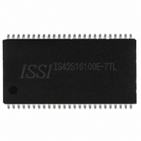
IS42S16100E-7TL ISSI, Integrated Silicon Solution Inc, IS42S16100E-7TL Datasheet - Page 32

IS42S16100E-7TL
Manufacturer Part Number
IS42S16100E-7TL
Description
IC SDRAM 16MBIT 143MHZ 50TSOP
Manufacturer
ISSI, Integrated Silicon Solution Inc
Type
SDRAMr
Specifications of IS42S16100E-7TL
Format - Memory
RAM
Memory Type
SDRAM
Memory Size
16M (1M x 16)
Speed
143MHz
Interface
Parallel
Voltage - Supply
3 V ~ 3.6 V
Operating Temperature
0°C ~ 70°C
Package / Case
50-TSOPII
Organization
1Mx16
Density
16Mb
Address Bus
12b
Access Time (max)
6/5.5ns
Maximum Clock Rate
143MHz
Operating Supply Voltage (typ)
3.3V
Package Type
TSOP-II
Operating Temp Range
0C to 70C
Operating Supply Voltage (max)
3.6V
Operating Supply Voltage (min)
3V
Supply Current
130mA
Pin Count
50
Mounting
Surface Mount
Operating Temperature Classification
Commercial
Lead Free Status / RoHS Status
Lead free / RoHS Compliant
Other names
706-1071
IS42S16100E-7TL
IS42S16100E-7TL
Available stocks
Company
Part Number
Manufacturer
Quantity
Price
Company:
Part Number:
IS42S16100E-7TL
Manufacturer:
ISSI
Quantity:
6 545
Company:
Part Number:
IS42S16100E-7TL
Manufacturer:
ISSI
Quantity:
851
Company:
Part Number:
IS42S16100E-7TLI
Manufacturer:
ISSI
Quantity:
11 200
Company:
Part Number:
IS42S16100E-7TLI
Manufacturer:
ISSI
Quantity:
104
Part Number:
IS42S16100E-7TLI
Manufacturer:
ISSI
Quantity:
20 000
IS42S16100E, IC42S16100E
Write Cycle Interruption Using the
Precharge Command
A write cycle can be interrupted by the execution of the
precharge command before that cycle completes. The
delay time (t
where burst input is invalid, i.e., the point where input data
is no longer written to device internal memory is zero clock
cycles regardless of the CAS.
To inhibit invalid write, the DQM signal must be asserted
HIGH with the precharge command.
This precharge command and burst write command must
be of the same bank, otherwise it is not precharge interrupt
but only another bank precharge of dual bank operation.
32
CAS latency = 2, burstlength = 4
CAS latency = 3, burstlength = 4
COMMAND
COMMAND
wdl
) from the precharge command to the point
CLK
DQ
DQM
CLK
DQ
WRITE (CA=A, BANK 0)
WRITE A0
D
IN
WRITE (CA=A, BANK 0)
A0
D
WRITE A0
IN
D
IN
A0
A1
D
IN
D
IN
A1
A2
D
IN
D
IN
A2
t
A3
DPL
Inversely, to write all the burst data to the device, the
precharge command must be executed after the write
data recovery period (t
precharge command must be executed on one clock
cycle that follows the input of the last burst data item.
PRECHARGE (BANK 0)
D
PRE 0
Integrated Silicon Solution, Inc. — www.issi.com
CAS Latency
PRE 0
IN
A3
t
MASKED BY DQM
t
wdl
dpl
PRECHARGE (BANK 0)
t
WDL
=0
dpl
) has elapsed. Therefore, the
3
0
1
2
0
1
01/22/08
Rev. C


