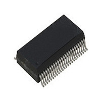
IDT74FCT164245TPVG IDT, Integrated Device Technology Inc, IDT74FCT164245TPVG Datasheet - Page 2

IDT74FCT164245TPVG
Manufacturer Part Number
IDT74FCT164245TPVG
Description
IC XLATOR TXRX 16BIT 48-SSOP
Manufacturer
IDT, Integrated Device Technology Inc
Series
74FCTr
Datasheet
1.IDT74FCT164245TPVG8.pdf
(8 pages)
Specifications of IDT74FCT164245TPVG
Logic Function
Translator, Bidirectional, 3-State
Number Of Bits
8
Input Type
Voltage
Output Type
Voltage
Number Of Channels
2
Number Of Outputs/channel
8
Differential - Input:output
No/No
Propagation Delay (max)
5ns
Voltage - Supply
2.7 V ~ 3.6 V
Operating Temperature
-40°C ~ 85°C
Package / Case
48-SSOP
Supply Voltage
2.7 V ~ 5.5 V
Data Rate
-
Logic Family
FCT
Operating Supply Voltage (typ)
3.3/5V
Propagation Delay Time
6.5ns
Number Of Elements
2
Input Logic Level
TTL
Output Logic Level
TTL
Package Type
SSOP
Polarity
Non-Inverting
Logical Function
Bus Transceiver with Voltage Translation
Operating Supply Voltage (min)
2.7/4.5V
Operating Supply Voltage (max)
3.6/5.5V
Quiescent Current (typ)
350uA
Technology
CMOS
Operating Temp Range
-40C to 85C
Operating Temperature Classification
Industrial
Mounting
Surface Mount
Pin Count
48
Lead Free Status / RoHS Status
Lead free / RoHS Compliant
Data Rate
-
Lead Free Status / Rohs Status
Lead free / RoHS Compliant
Other names
74FCT164245TPVG
Available stocks
Company
Part Number
Manufacturer
Quantity
Price
Company:
Part Number:
IDT74FCT164245TPVG8
Manufacturer:
PMC
Quantity:
129
PIN CONFIGURATION
POWER SUPPLY SEQUENCING
maintained at all times. For the range of V
+ 0.9V), both the A and B ports will remain in a High-Impedance state.
IDT74FCT164245T
FAST CMOS 16-BIT BIDIRECTIONAL 3.3V TO 5V TRANSLATOR
In the 74FCT164245T, the condition of V
GND
GND
GND
GND
1
V
V
2
DIR
DIR
1
1
1
1
CC1
1
1
1
1
2
2
2
2
CC1
2
2
2
2
B
B
B
B
B
B
B
B
B
B
B
B
B
B
B
B
1
2
3
4
5
6
7
8
1
2
3
4
5
6
7
8
1
2
3
4
5
6
7
8
9
10
11
12
13
14
15
16
17
18
19
20
21
22
23
24
SSOP/ TSSOP
TOP VIEW
CC1
= (V
40
35
CC1
48
47
46
45
44
43
42
41
39
38
37
36
34
33
32
31
30
29
28
27
26
25
CC2
≥ (V
– 0.5V) to V
CC2
1
1
1
GND
1
1
V
1
1
GND
1
1
2
2
GND
2
2
V
2
2
GND
2
2
2
– 0.5V) must be
OE
A
A
A
A
A
A
A
A
A
A
A
A
A
A
A
A
OE
CC2
CC2
1
2
3
4
5
6
7
8
1
2
3
4
5
6
7
8
CC1
= (V
CC2
2
CAPACITANCE
NOTE:
1. This parameter is measured at characterization but not tested.
ABSOLUTE MAXIMUM RATINGS
NOTES:
1. Stresses greater than those listed under ABSOLUTE MAXIMUM RATINGS may cause
2. All devices except Vcc
3. Power supply terminal Vcc
PIN DESCRIPTION
FUNCTION TABLE
NOTE:
1. H = HIGH Voltage Level
Symbol
V
V
T
T
T
P
I
Symbol
C
C
OUT
A
BIAS
STG
TERM
TERM
permanent damage to the device. This is a stress rating only and functional operation
of the device at these or any other conditions above those indicated in the operational
sections of this specification is not implied. Exposure to absolute maximum rating
conditions for extended periods may affect reliability.
T
IN
I/O
L = LOW Voltage Level
X = Don't Care
Z = High-Impedance
Pin Names
xOE
xDIR
xOE
x A x
x B x
H
(2)
(3)
L
L
Terminal Voltage with Respect to GND
Terminal Voltage with Respect to GND
Operating Temperature
Temperature Under Bias
Storage Temperature
Power Dissipation
DC Output Current
Inputs
Input Capacitance
I/O Capacitance
Parameter
xDIR
H
L
X
Output Enable Input (Active LOW)
Direction Control Input
Side A Inputs or 3-State Outputs (3.3V Port)
Side B Inputs or 3-State Outputs (5V Port)
2
Description
.
(1)
2
.
(T
INDUSTRIAL TEMPERATURE RANGE
Bus B Data to Bus A
Bus A Data to Bus B
High Z State
A
= +25°C, F = 1.0MHz)
Conditions
(1)
V
V
OUT
IN
Description
= 0V
= 0V
Outputs
–0.5 to Vcc
Typ.
3.5
3.5
–55 to +125
–55 to +125
–60 to +120
–40 to +85
–0.5 to +7
Max
1
Max.
1
+0.5
6
8
(1)
(1)
(1)
(1)
(1)
Unit
Unit
pF
pF
mA
° C
° C
° C
W
V
V


