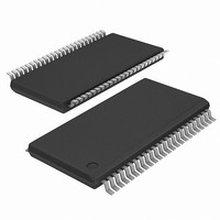
IDT74FCT163245APAG IDT, Integrated Device Technology Inc, IDT74FCT163245APAG Datasheet - Page 2

IDT74FCT163245APAG
Manufacturer Part Number
IDT74FCT163245APAG
Description
IC BI-DIR TRANSCVR 16BIT 48TSSOP
Manufacturer
IDT, Integrated Device Technology Inc
Series
74FCTr
Datasheet
1.IDT74FCT163245CPAG.pdf
(7 pages)
Specifications of IDT74FCT163245APAG
Logic Function
Translator, Bidirectional, 3-State
Number Of Bits
8
Input Type
Voltage
Output Type
Voltage
Number Of Channels
2
Number Of Outputs/channel
8
Differential - Input:output
No/No
Propagation Delay (max)
4.6ns
Voltage - Supply
2.7 V ~ 3.6 V
Operating Temperature
-40°C ~ 85°C
Package / Case
*
Supply Voltage
*
Logic Family
FCT
Operating Supply Voltage (typ)
3.3V
Propagation Delay Time
6.2ns
Number Of Elements
2
Input Logic Level
TTL
Output Logic Level
TTL
Package Type
TSSOP
Polarity
Non-Inverting
Logical Function
Bus Transceiver
Operating Supply Voltage (min)
2.7V
Quiescent Current (typ)
100nA
Technology
CMOS
Operating Temp Range
-40C to 85C
Operating Temperature Classification
Industrial
Mounting
Surface Mount
Pin Count
48
Data Rate
-
Lead Free Status / RoHS Status
Lead free / RoHS Compliant
Data Rate
-
Lead Free Status / Rohs Status
Compliant
Other names
74FCT163245APAG
PIN CONFIGURATION
IDT74FCT163245A/C
3.3V CMOS 16-BIT BIDIRECTIONAL TRANSCEIVER
GND
GND
GND
GND
1
2
DIR
V
V
DIR
1
1
1
1
1
1
1
1
2
2
2
2
2
2
2
2
B
B
B
B
CC
B
B
B
B
B
B
B
B
CC
B
B
B
B
1
2
3
4
5
6
7
8
1
2
3
4
5
6
7
8
SSOP/ TSSOP/ TVSOP
1
2
3
4
5
6
7
8
9
10
11
12
13
14
15
16
17
18
19
20
21
22
23
24
TOP VIEW
40
35
48
47
46
45
44
43
42
41
39
38
37
36
34
33
32
31
30
29
28
27
26
25
GND
GND
GND
GND
1
1
1
1
1
V
1
1
1
1
2
2
2
2
V
2
2
2
2
2
OE
A
A
A
A
A
A
A
A
A
A
A
A
A
A
A
A
OE
CC
CC
1
2
3
4
5
6
7
8
1
2
3
4
5
6
7
8
2
CAPACITANCE
NOTE:
1. This parameter is measured at characterization but not tested.
FUNCTION TABLE
ABSOLUTE MAXIMUM RATINGS
NOTES:
1. Stresses greater than those listed under ABSOLUTE MAXIMUM RATINGS may cause
2. Vcc terminals.
3. Input terminals.
4. Outputs and I/O terminals.
PIN DESCRIPTION
NOTE:
1. H = HIGH Voltage Level
Symbol
V
V
V
T
I
Symbol
C
C
OUT
STG
TERM
TERM
TERM
permanent damage to the device. This is a stress rating only and functional operation
of the device at these or any other conditions above those indicated in the operational
sections of this specification is not implied. Exposure to absolute maximum rating
conditions for extended periods may affect reliability.
L = LOW Voltage Level
X = Don't Care
Z = High-impedance
IN
OUT
Pin Names
xOE
xDIR
xOE
H
x A x
x B x
L
L
(2)
(3)
(4)
1
Inputs
Terminal Voltage with Respect to GND
Terminal Voltage with Respect to GND
Terminal Voltage with Respect to GND
Storage Temperature
DC Output Current
Input Capacitance
Output Capacitance
Parameter
xDIR
H
L
X
Output Enable Input (Active LOW)
Direction Control Input
Side A Inputs or 3-State Outputs
Side B Inputs or 3-State Outputs
Description
(1)
(T
INDUSTRIAL TEMPERATURE RANGE
A
= +25°C, F = 1.0MHz)
(1)
Conditions
V
V
Bus B Data to Bus A
Bus A Data to Bus B
High Z State
OUT
IN
Description
= 0V
= 0V
Outputs
–0.5 to V
Typ.
3.5
3.5
–0.5 to +4.6
–65 to +150
–60 to +60
–0.5 to 7
Max
CC
Max.
+0.5
6
8
(1)
(1)
(1)
(1)
(1)
Unit
Unit
pF
pF
mA
° C
V
V
V


