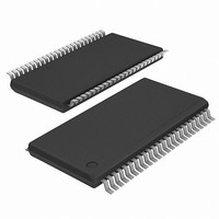
SSTVF16857AG IDT, Integrated Device Technology Inc, SSTVF16857AG Datasheet - Page 2

SSTVF16857AG
Manufacturer Part Number
SSTVF16857AG
Description
IC DDR REGISTER 48-TSSOP
Manufacturer
IDT, Integrated Device Technology Inc
Series
74SSTVFr
Specifications of SSTVF16857AG
Logic Type
Registered Buffer with SSTL_2 Inputs and Outputs
Supply Voltage
2.3 V ~ 2.7 V
Number Of Bits
14
Operating Temperature
0°C ~ 70°C
Mounting Type
Surface Mount
Package / Case
48-TSSOP
Lead Free Status / RoHS Status
Contains lead / RoHS non-compliant
Available stocks
Company
Part Number
Manufacturer
Quantity
Price
Company:
Part Number:
SSTVF16857AG
Manufacturer:
HARRIS
Quantity:
22 805
Part Number:
SSTVF16857AGLF
Manufacturer:
IDT
Quantity:
20 000
Company:
Part Number:
SSTVF16857AGT
Manufacturer:
ICS
Quantity:
2 528
ICSSSTVF16857
Advance Information
0746—10/28/02
General Description
Pin Configuration
The 14-bit ICSSSTVF16857 is a universal bus driver designed for 2.3V to 2.7V V
except for the LVCMOS RESET# input.
Data flow from D to Q is controlled by the differential clock (CLK/CLK#) and a control signal (RESET#). The positive edge
of CLK is used to trigger the data flow and CLK# is used to maintain sufficient noise margins where as RESET#, an
LVCMOS asynchronous signal, is intended for use at the time of power-up only. ICSSSTVF16857 supports low-power
standby operation. A logic level “Low” at RESET# assures that all internal registers and outputs (Q) are reset to the logic
“Low” state, and all input receivers, data (D) and clock (CLK/CLK#) are switched off. Please note that RESET# must always
be supported with LVCMOS levels at a valid logic state because VREF may not be stable during power-up.
To ensure that outputs are at a defined logic state before a stable clock has been supplied, RESET# must be held at a logic
“Low” level during power up.
In the DDR DIMM application, RESET# is specified to be completely asynchronous with respect to CLK and CLK#.
Therefore, no timing relationship can be guaranteed between the two signals. When entering a low-power standby state,
the register will be cleared and the outputs will be driven to a logic “Low” level quickly relative to the time to disable the
differential input receivers. This ensures there are no glitches on the output. However, when coming out of low-power
standby state, the register will become active quickly relative to the time to enable the differential input receivers. When
the data inputs are at a logic level “Low” and the clock is stable during the “Low”-to-”High” transition of RESET# until the
input receivers are fully enabled, the design ensures that the outputs will remain at a logic “Low” level.
2
2
3
1
, 4
, 5
, 2
, 4
, 5
P
4
, 3
, 3
N I
2
2
3
2
2
, 9
1
, 6
, 3
, 6
, 3
, 7
, 8
, 8
, 4
4
N
1
, 4
, 5
2
2
4
3
3
3
3
3
3
U
, 2
1
1
, 0
, 9
, 0
, 6
8
9
, 7
4
5
, 3
, 1
M
4
, 2
1
, 7
1
3
4
B
4
4
, 6
2
1
1
, 9
, 0
, 1
6
5
E
, 0
, 2
4
2
R
8
1
3
4
1
, 7
, 8
, 1
, 2
P
R
Q
N I
D
V
V
C
E
G
V
C
1 (
D
1 (
R
L
S
N
D
N
L
D
K
E
: 4
: 4
E
A
K
D
D
Q
#
F
T
) 1
M
) 1
#
E
O
N I
N I
N I
N I
N I
T
U
P
P
P
Y
T
W
W
P
P
P
W
P
P
P
P
U
U
U
U
U
R
R
R
E
U
T
T
T
T
T
T
D
D
P
N
R
n I
G
O
C
2
o
a
a
e
e
o
o r
u
p
s
a t
a t
g
e r
s
p t
t u
i t i
u
t e
a
n
t u
o
n i
e v
i t
s
e r
d
e v
a (
u
u
p
s
e f
p t
p
c
t u
i t c
u
p
e r
o l
c
t u
p
y l
o l
e v
p
k c
n
k c
y l
c
v
o l
e
l o
n i
v
n i
w
a t
l o
v
p
l o
p
t u
)
a t
g
t u
a t
e
g
g
e
D
e
DD
E
S
operation and SSTL_2 I/O levels,
C
R
P I
I T
O
N


