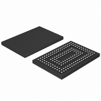
SSTUA32S865ET/G;55 NXP Semiconductors, SSTUA32S865ET/G;55 Datasheet - Page 9

SSTUA32S865ET/G;55
Manufacturer Part Number
SSTUA32S865ET/G;55
Description
IC BUFFER 1.8V 28BIT SOT802
Manufacturer
NXP Semiconductors
Datasheet
1.SSTUA32S865ETG51.pdf
(29 pages)
Specifications of SSTUA32S865ET/G;55
Logic Type
1:2 Registered Buffer with Parity
Supply Voltage
1.7 V ~ 2 V
Number Of Bits
28
Operating Temperature
0°C ~ 70°C
Mounting Type
Surface Mount
Package / Case
160-TFBGA
Lead Free Status / RoHS Status
Lead free / RoHS Compliant
Other names
935279445557
SSTUA32S865ET/G
SSTUA32S865ET/G
SSTUA32S865ET/G
SSTUA32S865ET/G
NXP Semiconductors
[2]
[3]
SSTUA32S865_2
Product data sheet
This condition assumes PTYERR is HIGH at the crossing of CK going HIGH and CK going LOW. If PTYERR is LOW, it stays latched
LOW for two clock cycles or until RESET is driven LOW.
CSGATEEN is ‘don’t care’ for PTYERR.
PTYERR
0
is the previous state of output PTYERR.
7.2 Functional information
This 28-bit 1 : 2 registered buffer with parity is designed for 1.7 V to 2.0 V V
All clock and data inputs are compatible with the JEDEC standard for SSTL_18. The
control inputs are LVCMOS. All outputs are 1.8 V CMOS drivers that have been optimized
to drive the DDR2 DIMM load.
The SSTUA32S865 operates from a differential clock (CK and CK). Data are registered at
the crossing of CK going HIGH, and CK going LOW.
The device supports low-power standby operation. When the reset input (RESET) is LOW,
the differential input receivers are disabled, and undriven (floating) data, clock and
reference voltage (VREF) inputs are allowed. In addition, when RESET is LOW all
registers are reset, and all outputs except PTYERR are forced LOW. The LVCMOS
RESET input must always be held at a valid logic HIGH or LOW level.
To ensure defined outputs from the register before a stable clock has been supplied,
RESET must be held in the LOW state during power-up.
In the DDR2 RDIMM application, RESET is specified to be completely asynchronous with
respect to CK and CK. Therefore, no timing relationship can be guaranteed between the
two. When entering reset, the register will be cleared and the data outputs will be driven
LOW quickly, relative to the time to disable the differential input receivers. However, when
coming out of reset, the register will become active quickly, relative to the time to enable
the differential input receivers. As long as the data inputs are LOW, and the clock is stable
during the time from the LOW-to-HIGH transition of RESET until the input receivers are
fully enabled, the design of the SSTUA32S865 ensures that the outputs remain LOW, thus
ensuring no glitches on the output.
The device monitors both DCS0 and DCS1 inputs and will gate the Qn outputs from
changing states when both DCS0 and DCS1 are HIGH. If either DCS0 or DCS1 input is
LOW, the Qn outputs will function normally. The RESET input has priority over the DCS0
and DCS1 control and will force the Qn outputs LOW and the PTYERR output HIGH. If the
DCSn-control functionality is not desired, then the CSGATEEN input can be hardwired to
ground, in which case, the setup-time requirement for DCSn would be the same as for the
other Dn data inputs.
The SSTUA32S865 includes a parity checking function. The SSTUA32S865 accepts a
parity bit from the memory controller at its input pin PARIN, compares it with the data
received on the Dn inputs (with either DCS0 or DCS1 active) and indicates whether a
parity error has occurred on its open-drain PTYERR pin (active LOW).
Rev. 02 — 16 March 2007
1.8 V DDR2-667 registered buffer with parity
SSTUA32S865
© NXP B.V. 2007. All rights reserved.
DD
operation.
9 of 29


