SSTUM32866EC/S,518 NXP Semiconductors, SSTUM32866EC/S,518 Datasheet - Page 9
SSTUM32866EC/S,518
Manufacturer Part Number
SSTUM32866EC/S,518
Description
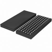
IC BUFFER 1.8V 25BIT 96-LFBGA
Manufacturer
NXP Semiconductors
Datasheet
1.SSTUM32866ECS518.pdf
(28 pages)
Specifications of SSTUM32866EC/S,518
Logic Type
1:1, 1:2 Configurable Registered Buffer with Parity
Supply Voltage
1.7 V ~ 2 V
Number Of Bits
25, 14
Operating Temperature
0°C ~ 85°C
Mounting Type
Surface Mount
Package / Case
96-LFBGA
Logic Family
SSTU
Logical Function
Registered Buffer
Number Of Elements
1
Number Of Inputs
25
Number Of Outputs
25
High Level Output Current
-8mA
Low Level Output Current
8mA
Package Type
LFBGA
Propagation Delay Time
3ns
Operating Supply Voltage (typ)
1.8V
Operating Supply Voltage (max)
2V
Operating Supply Voltage (min)
1.7V
Clock-edge Trigger Type
Posit/Negat-Edge
Polarity
Non-Inverting
Technology
CMOS
Mounting
Surface Mount
Pin Count
96
Operating Temp Range
0C to 85C
Operating Temperature Classification
Commercial
Lead Free Status / RoHS Status
Lead free / RoHS Compliant
Other names
935284578518
SSTUM32866EC/S-T
SSTUM32866EC/S-T
SSTUM32866EC/S-T
SSTUM32866EC/S-T
Available stocks
Company
Part Number
Manufacturer
Quantity
Price
Company:

Part Number:
SSTUM32866EC/S,518
Manufacturer:
NXP Semiconductors
Quantity:
10 000


NXP Semiconductors
Table 4.
L = LOW voltage level; H = HIGH voltage level; X = don’t care;
[1]
SSTUM32866_1
Product data sheet
RESET
Q
H
H
H
H
H
H
H
H
H
H
H
H
L
0
is the previous state of the associated output.
Function table (each flip-flop)
X or floating
DCS
7.1 Function table
H
H
H
H
H
H
L
L
L
L
L
L
The device also supports low-power active operation by monitoring both system chip
select (DCS and CSR) inputs and will gate the Qn and PPO outputs from changing states
when both DCS and CSR inputs are HIGH. If either DCS or CSR input is LOW, the Qn
and PPO outputs will function normally. The RESET input has priority over the DCS and
CSR control and when driven LOW will force the Qn and PPO outputs LOW, and the
QERR output HIGH. If the DCS control functionality is not desired, then the CSR input can
be hard-wired to ground, in which case, the setup time requirement for DCS would be the
same as for the other Dn data inputs. To control the low-power mode with DCS only, then
the CSR input should be pulled up to V
To ensure defined outputs from the register before a stable clock has been supplied,
RESET must be held in the LOW state during power-up.
In the DDR2 RDIMM application, RESET is specified to be completely asynchronous with
respect to CK and CK. Therefore, no timing relationship can be guaranteed between the
two. When entering reset, the register will be cleared and the Qn outputs will be driven
LOW quickly, relative to the time to disable the differential input receivers. However, when
coming out of reset, the register will become active quickly, relative to the time to enable
the differential input receivers. As long as the data inputs are LOW, and the clock is stable
during the time from the LOW-to-HIGH transition of RESET until the input receivers are
fully enabled, the design of the SSTUM32866 must ensure that the outputs will remain
LOW, thus ensuring no glitches on the output.
X or floating
CSR
H
H
H
H
H
H
L
L
L
L
L
L
Inputs
X or floating
L or H
L or H
L or H
L or H
CK
Rev. 01 — 29 June 2007
1.8 V DDR2-1G configurable registered buffer with parity
X or floating
L or H
L or H
L or H
L or H
CK
= LOW-to-HIGH transition;
DD
through a pull-up resistor.
Dn, DODTn,
X or floating
DCKEn
H
X
H
X
H
X
H
X
L
L
L
L
Qn
Q
Q
Q
Q
Q
Q
H
H
H
L
L
L
L
SSTUM32866
0
0
0
0
0
0
= HIGH-to-LOW transition.
Outputs
QCS
Q
Q
Q
Q
© NXP B.V. 2007. All rights reserved.
H
H
H
H
L
L
L
L
L
0
0
0
0
[1]
QODT,
QCKE
Q
Q
Q
Q
H
H
H
H
L
L
L
L
L
9 of 28
0
0
0
0
Related parts for SSTUM32866EC/S,518
Image
Part Number
Description
Manufacturer
Datasheet
Request
R

Part Number:
Description:
Sstum32866 1.8 V 25-bit 1 1 Or 14-bit 1 2 Configurable Registered Buffer With Parity For Ddr2-1g Rdimm Applications
Manufacturer:
NXP Semiconductors
Datasheet:
Part Number:
Description:
NXP Semiconductors designed the LPC2420/2460 microcontroller around a 16-bit/32-bitARM7TDMI-S CPU core with real-time debug interfaces that include both JTAG andembedded trace
Manufacturer:
NXP Semiconductors
Datasheet:

Part Number:
Description:
NXP Semiconductors designed the LPC2458 microcontroller around a 16-bit/32-bitARM7TDMI-S CPU core with real-time debug interfaces that include both JTAG andembedded trace
Manufacturer:
NXP Semiconductors
Datasheet:
Part Number:
Description:
NXP Semiconductors designed the LPC2468 microcontroller around a 16-bit/32-bitARM7TDMI-S CPU core with real-time debug interfaces that include both JTAG andembedded trace
Manufacturer:
NXP Semiconductors
Datasheet:
Part Number:
Description:
NXP Semiconductors designed the LPC2470 microcontroller, powered by theARM7TDMI-S core, to be a highly integrated microcontroller for a wide range ofapplications that require advanced communications and high quality graphic displays
Manufacturer:
NXP Semiconductors
Datasheet:
Part Number:
Description:
NXP Semiconductors designed the LPC2478 microcontroller, powered by theARM7TDMI-S core, to be a highly integrated microcontroller for a wide range ofapplications that require advanced communications and high quality graphic displays
Manufacturer:
NXP Semiconductors
Datasheet:
Part Number:
Description:
The Philips Semiconductors XA (eXtended Architecture) family of 16-bit single-chip microcontrollers is powerful enough to easily handle the requirements of high performance embedded applications, yet inexpensive enough to compete in the market for hi
Manufacturer:
NXP Semiconductors
Datasheet:
Part Number:
Description:
The XA-S3 device is a member of Philips Semiconductors? XA(eXtended Architecture) family of high performance 16-bitsingle-chip microcontrollers
Manufacturer:
NXP Semiconductors
Datasheet:

Part Number:
Description:
The NXP BlueStreak LH75401/LH75411 family consists of two low-cost 16/32-bit System-on-Chip (SoC) devices
Manufacturer:
NXP Semiconductors
Datasheet:
Part Number:
Description:
The NXP LPC3130/3131 combine an 180 MHz ARM926EJ-S CPU core, high-speed USB2
Manufacturer:
NXP Semiconductors
Datasheet:
Part Number:
Description:
The NXP LPC3141 combine a 270 MHz ARM926EJ-S CPU core, High-speed USB 2
Manufacturer:
NXP Semiconductors
Part Number:
Description:
The NXP LPC3143 combine a 270 MHz ARM926EJ-S CPU core, High-speed USB 2
Manufacturer:
NXP Semiconductors

Part Number:
Description:
The NXP LPC3152 combines an 180 MHz ARM926EJ-S CPU core, High-speed USB 2
Manufacturer:
NXP Semiconductors
Part Number:
Description:
The NXP LPC3154 combines an 180 MHz ARM926EJ-S CPU core, High-speed USB 2
Manufacturer:
NXP Semiconductors