SSTUM32866EC/S,518 NXP Semiconductors, SSTUM32866EC/S,518 Datasheet - Page 26
SSTUM32866EC/S,518
Manufacturer Part Number
SSTUM32866EC/S,518
Description
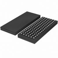
IC BUFFER 1.8V 25BIT 96-LFBGA
Manufacturer
NXP Semiconductors
Datasheet
1.SSTUM32866ECS518.pdf
(28 pages)
Specifications of SSTUM32866EC/S,518
Logic Type
1:1, 1:2 Configurable Registered Buffer with Parity
Supply Voltage
1.7 V ~ 2 V
Number Of Bits
25, 14
Operating Temperature
0°C ~ 85°C
Mounting Type
Surface Mount
Package / Case
96-LFBGA
Logic Family
SSTU
Logical Function
Registered Buffer
Number Of Elements
1
Number Of Inputs
25
Number Of Outputs
25
High Level Output Current
-8mA
Low Level Output Current
8mA
Package Type
LFBGA
Propagation Delay Time
3ns
Operating Supply Voltage (typ)
1.8V
Operating Supply Voltage (max)
2V
Operating Supply Voltage (min)
1.7V
Clock-edge Trigger Type
Posit/Negat-Edge
Polarity
Non-Inverting
Technology
CMOS
Mounting
Surface Mount
Pin Count
96
Operating Temp Range
0C to 85C
Operating Temperature Classification
Commercial
Lead Free Status / RoHS Status
Lead free / RoHS Compliant
Other names
935284578518
SSTUM32866EC/S-T
SSTUM32866EC/S-T
SSTUM32866EC/S-T
SSTUM32866EC/S-T
Available stocks
Company
Part Number
Manufacturer
Quantity
Price
Company:

Part Number:
SSTUM32866EC/S,518
Manufacturer:
NXP Semiconductors
Quantity:
10 000


NXP Semiconductors
14. Abbreviations
15. Revision history
Table 15.
SSTUM32866_1
Product data sheet
Document ID
SSTUM32866_1
Revision history
Release date
20070629
For further information on temperature profiles, refer to Application Note AN10365
“Surface mount reflow soldering description” .
Table 14.
Acronym
CMOS
DDR
DIMM
DUT
LVCMOS
PPO
PRR
RDIMM
SSTL
Fig 28. Temperature profiles for large and small components
MSL: Moisture Sensitivity Level
temperature
Abbreviations
Data sheet status
Product data sheet
Description
Complementary Metal Oxide Semiconductor
Double Data Rate
Dual In-line Memory Module
Device Under Test
Low Voltage Complementary Metal Oxide Semiconductor
Partial Parity Out
Pulse Repetition Rate
Registered Dual In-line Memory Module
Stub Series Terminated Logic
Rev. 01 — 29 June 2007
= minimum soldering temperature
1.8 V DDR2-1G configurable registered buffer with parity
maximum peak temperature
minimum peak temperature
= MSL limit, damage level
Change notice
-
SSTUM32866
temperature
Supersedes
-
peak
© NXP B.V. 2007. All rights reserved.
001aac844
time
26 of 28
Related parts for SSTUM32866EC/S,518
Image
Part Number
Description
Manufacturer
Datasheet
Request
R

Part Number:
Description:
Sstum32866 1.8 V 25-bit 1 1 Or 14-bit 1 2 Configurable Registered Buffer With Parity For Ddr2-1g Rdimm Applications
Manufacturer:
NXP Semiconductors
Datasheet:
Part Number:
Description:
NXP Semiconductors designed the LPC2420/2460 microcontroller around a 16-bit/32-bitARM7TDMI-S CPU core with real-time debug interfaces that include both JTAG andembedded trace
Manufacturer:
NXP Semiconductors
Datasheet:

Part Number:
Description:
NXP Semiconductors designed the LPC2458 microcontroller around a 16-bit/32-bitARM7TDMI-S CPU core with real-time debug interfaces that include both JTAG andembedded trace
Manufacturer:
NXP Semiconductors
Datasheet:
Part Number:
Description:
NXP Semiconductors designed the LPC2468 microcontroller around a 16-bit/32-bitARM7TDMI-S CPU core with real-time debug interfaces that include both JTAG andembedded trace
Manufacturer:
NXP Semiconductors
Datasheet:
Part Number:
Description:
NXP Semiconductors designed the LPC2470 microcontroller, powered by theARM7TDMI-S core, to be a highly integrated microcontroller for a wide range ofapplications that require advanced communications and high quality graphic displays
Manufacturer:
NXP Semiconductors
Datasheet:
Part Number:
Description:
NXP Semiconductors designed the LPC2478 microcontroller, powered by theARM7TDMI-S core, to be a highly integrated microcontroller for a wide range ofapplications that require advanced communications and high quality graphic displays
Manufacturer:
NXP Semiconductors
Datasheet:
Part Number:
Description:
The Philips Semiconductors XA (eXtended Architecture) family of 16-bit single-chip microcontrollers is powerful enough to easily handle the requirements of high performance embedded applications, yet inexpensive enough to compete in the market for hi
Manufacturer:
NXP Semiconductors
Datasheet:
Part Number:
Description:
The XA-S3 device is a member of Philips Semiconductors? XA(eXtended Architecture) family of high performance 16-bitsingle-chip microcontrollers
Manufacturer:
NXP Semiconductors
Datasheet:

Part Number:
Description:
The NXP BlueStreak LH75401/LH75411 family consists of two low-cost 16/32-bit System-on-Chip (SoC) devices
Manufacturer:
NXP Semiconductors
Datasheet:
Part Number:
Description:
The NXP LPC3130/3131 combine an 180 MHz ARM926EJ-S CPU core, high-speed USB2
Manufacturer:
NXP Semiconductors
Datasheet:
Part Number:
Description:
The NXP LPC3141 combine a 270 MHz ARM926EJ-S CPU core, High-speed USB 2
Manufacturer:
NXP Semiconductors
Part Number:
Description:
The NXP LPC3143 combine a 270 MHz ARM926EJ-S CPU core, High-speed USB 2
Manufacturer:
NXP Semiconductors

Part Number:
Description:
The NXP LPC3152 combines an 180 MHz ARM926EJ-S CPU core, High-speed USB 2
Manufacturer:
NXP Semiconductors
Part Number:
Description:
The NXP LPC3154 combines an 180 MHz ARM926EJ-S CPU core, High-speed USB 2
Manufacturer:
NXP Semiconductors