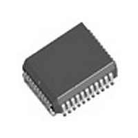
IDT728981J IDT, Integrated Device Technology Inc, IDT728981J Datasheet - Page 3

IDT728981J
Manufacturer Part Number
IDT728981J
Description
IC DGTL SW 256X256 44-PLCC
Manufacturer
IDT, Integrated Device Technology Inc
Series
7200r
Type
Multiplexerr
Datasheet
1.IDT728981JG.pdf
(10 pages)
Specifications of IDT728981J
Circuit
1 x 4:4
Independent Circuits
1
Voltage Supply Source
Single Supply
Voltage - Supply
4.75 V ~ 5.25 V
Operating Temperature
-40°C ~ 85°C
Mounting Type
Surface Mount
Package / Case
44-PLCC
Lead Free Status / RoHS Status
Contains lead / RoHS non-compliant
Current - Output High, Low
-
Lead Free Status / RoHS Status
Not Compliant, Contains lead / RoHS non-compliant
Other names
728981J
Available stocks
Company
Part Number
Manufacturer
Quantity
Price
Company:
Part Number:
IDT728981J
Manufacturer:
IDT, Integrated Device Technology Inc
Quantity:
10 000
Company:
Part Number:
IDT728981J8
Manufacturer:
IDT, Integrated Device Technology Inc
Quantity:
10 000
Company:
Part Number:
IDT728981JG
Manufacturer:
IDT, Integrated Device Technology Inc
Quantity:
10 000
Company:
Part Number:
IDT728981JG8
Manufacturer:
IDT, Integrated Device Technology Inc
Quantity:
10 000
Memory or Connection Memory. The Connection Memory is 16 bits wide and
is split into two 8-bit blocks—Connection Memory HIGH and Connection
Memory LOW. Each location in Connection Memory is associated with a
particular channel in an output stream so as to provide a one-to-one correspon-
dence between Connection and Data Memories. This correspondence allows
for per channel control for each TX output stream.
Memory Low and originates from the microprocessor (Figure 2). Where as in
Connection Mode (Figure 1), data is read from Data Memory using the address
in Connection Memory. Data destined for a particular channel on the serial
output stream is read during the previous channel time slot to allow time for
memory access and internal parallel-to-serial conversion.
CONNECTION MODE
are stored in the Connection Memory Low. The Connection Memory Low
locations are mapped to corresponding 8-bit x 32-channel output. The contents
of the Data Memory at the selected address are then transferred to the parallel-
to-serial converters. By having the output channel to specify the input channel
through the Connection Memory, input channels can be broadcast to several
output channels.
PROCESSOR MODE
locations which are to be output on the TX streams. The contents of the
Connection Memory Low are transferred to the parallel-to-serial converter one
channel before it is to be output and are transmitted each frame to the output until
it is changed by the CPU.
CONTROL
functions available in the IDT728981. Output channels are selected into specific
RX
IDT728981 Time Slot Interchange
Digital Switch 128 x 128
Data to be output on the serial streams may come from two sources: Data
In Processor Mode, data output on the TX is taken from the Connection
In Connection Mode, the addresses of input source for all output channels
In Processor Mode the CPU writes data to specific Connection Memory Low
The Connection Memory High bits (Table 4) control the per-channel
Serial Data
Serial Data
Receive
Streams
Receive
Streams
Figure 1. Connection Mode
Figure 2. Processor Mode
Microprocessor
Connection
Connection
Memory
Memory
Memory
Data
Memory
Data
Serial Data
Transmit
Streams
Serial Data
Transmit
Streams
5703 drw06
5703 drw05
TX
TX
3
modes such as: Processor mode or Connection mode and Output Drivers
Enabled or in three-state condition.
OUTPUT DRIVE ENABLE (ODE)
is held LOW all TX outputs will be placed in high impedance regardless
Connection Memory High programming. However, if ODE is HIGH, the contents
of Connection Memory High control the output state on a per-channel basis.
DELAY THROUGH THE IDT728981
streams results in a delay through the device. The delay through the IDT728981
device varies according to the combination of input and output streams and the
movement within the stream from channel to channel. Data received on an input
stream must first be stored in Data Memory before it is sent out.
serial-to-parallel converter. Likewise, before data leaves the device, it must
pass through the internal parallel-to-serial converter. This data preparation has
an effect on the channel positioning in the frame immediately following the
incoming frame—mainly, data cannot leave in the same time slot. Therefore,
information that is to be output in the same channel position as the information
is input, relative to the frame pulse, will be output in the following frame.
information entered the IDT728981 depends on which RX stream the channel
information enters on and which TX stream the information leaves on. This is
caused by the order in which input stream information is placed into Data Memory
and the order in which stream information is queued for output. Table 1 shows the
allowable input/output stream combinations for the minimum two channel delay.
NOTES:
1. Writing to the Control Register is the only fast transaction.
2. Memory and stream are specified by the contents of the Control Register.
Table 1. Input Stream to Output Stream Combinations that can Provide the
A5 A4 A3 A2 A1 A0
0
1
1
1
1
1
·
The ODE pin is the master three-state output control pin. If the ODE input
The transfer of information from the input serial streams to the output serial
As information enters the IDT728981 it must first pass through an internal
Whether information can be output during a following timeslot after the
X
0
0
1
Input
X
0
0
1
0
1
X
0
0
1
0
0
0
1
Table 2. Address Mapping
Minimum 2-Channel Delay
0
0
1
1
HEX ADDRESS
C
ommercial Temperature Range
00-1F
20
21
3F
Output Stream
1,2,3
3
Control Register
Channel 31
Channel 0
Channel 1
LOCATION
(2)
(2)
(2)
(1)


