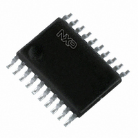
74LVC373APW,118 NXP Semiconductors, 74LVC373APW,118 Datasheet - Page 4

74LVC373APW,118
Manufacturer Part Number
74LVC373APW,118
Description
IC OCTAL TRANSP LATCH 20-TSSOP
Manufacturer
NXP Semiconductors
Series
74LVCr
Type
D-Typer
Datasheet
1.74LVC373APW118.pdf
(20 pages)
Specifications of 74LVC373APW,118
Logic Type
D-Type Transparent Latch
Package / Case
20-TSSOP
Circuit
8:8
Output Type
Tri-State
Voltage - Supply
2.7 V ~ 3.6 V
Independent Circuits
1
Delay Time - Propagation
1.5ns
Current - Output High, Low
24mA, 24mA
Operating Temperature
-40°C ~ 125°C
Mounting Type
Surface Mount
Number Of Circuits
8
Logic Family
74LVC
Polarity
Non-Inverting
Input Bias Current (max)
0.1 uA
High Level Output Current
- 24 mA
Low Level Output Current
24 mA
Propagation Delay Time
9 ns
Supply Voltage (max)
3.6 V
Supply Voltage (min)
1.2 V
Maximum Operating Temperature
+ 125 C
Minimum Operating Temperature
- 40 C
Mounting Style
SMD/SMT
Number Of Bits
8
Number Of Elements
1
Latch Mode
Transparent
Technology
CMOS
Package Type
TSSOP
Operating Supply Voltage (typ)
1.8/2.5/3.3V
Operating Supply Voltage (min)
1.2V
Operating Supply Voltage (max)
3.6V
Operating Temp Range
-40C to 125C
Operating Temperature Classification
Automotive
Mounting
Surface Mount
Pin Count
20
Lead Free Status / RoHS Status
Lead free / RoHS Compliant
Lead Free Status / RoHS Status
Lead free / RoHS Compliant, Lead free / RoHS Compliant
Other names
568-2304-2
74LVC373APW-T
935218650118
74LVC373APW-T
935218650118
Available stocks
Company
Part Number
Manufacturer
Quantity
Price
Company:
Part Number:
74LVC373APW,118
Manufacturer:
NXP Semiconductors
Quantity:
1 850
Philips Semiconductors
2003 May 19
handbook, halfpage
handbook, halfpage
Octal D-type transparent latch with
5 V tolerant inputs/outputs; 3-state
(1) The die substrate is attached to this pad using conductive die
attach material. It can not be used as a supply pin or input.
Fig.1 Pin configuration DHVQFN20.
Q0
D0
D1
Q1
Q2
D2
D3
Q3
Top view
18
17
14
13
8
7
4
3
2
3
4
5
6
7
8
9
Fig.3 Logic symbol.
D7
D6
D5
D4
D3
D2
D1
D0
LE
11
GND
1OE
10
GND
1
OE
1
Q7
Q6
Q5
Q4
Q3
Q2
Q1
Q0
V CC
(1)
11
LE
20
MNA881
19
16
15
12
9
6
5
2
MDB199
19
18
17
16
15
14
13
12
Q7
D7
D6
Q6
Q5
D5
D4
Q4
4
andbook, halfpage
handbook, halfpage
Fig.2 Pin configuration SO20 and (T)SSOP20.
Fig.4 Logic symbol (IEEE/IEC).
GND
13
14
17
18
11
OE
Q0
Q1
Q2
Q3
D0
D1
D2
D3
1
3
4
7
8
10
1
2
3
4
5
6
7
8
9
1D
EN
C1
373A
MNA880
MNA879
15
14
13
12
19
18
17
16
11
20
12
15
16
19
Product specification
2
5
6
9
74LVC373A
V CC
Q7
D7
D6
Q6
Q5
D5
D4
Q4
LE


