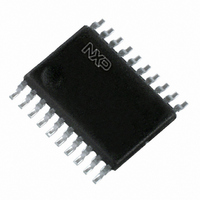
74LVC373APW,118 NXP Semiconductors, 74LVC373APW,118 Datasheet - Page 11

74LVC373APW,118
Manufacturer Part Number
74LVC373APW,118
Description
IC OCTAL TRANSP LATCH 20-TSSOP
Manufacturer
NXP Semiconductors
Series
74LVCr
Type
D-Typer
Datasheet
1.74LVC373APW118.pdf
(20 pages)
Specifications of 74LVC373APW,118
Logic Type
D-Type Transparent Latch
Package / Case
20-TSSOP
Circuit
8:8
Output Type
Tri-State
Voltage - Supply
2.7 V ~ 3.6 V
Independent Circuits
1
Delay Time - Propagation
1.5ns
Current - Output High, Low
24mA, 24mA
Operating Temperature
-40°C ~ 125°C
Mounting Type
Surface Mount
Number Of Circuits
8
Logic Family
74LVC
Polarity
Non-Inverting
Input Bias Current (max)
0.1 uA
High Level Output Current
- 24 mA
Low Level Output Current
24 mA
Propagation Delay Time
9 ns
Supply Voltage (max)
3.6 V
Supply Voltage (min)
1.2 V
Maximum Operating Temperature
+ 125 C
Minimum Operating Temperature
- 40 C
Mounting Style
SMD/SMT
Number Of Bits
8
Number Of Elements
1
Latch Mode
Transparent
Technology
CMOS
Package Type
TSSOP
Operating Supply Voltage (typ)
1.8/2.5/3.3V
Operating Supply Voltage (min)
1.2V
Operating Supply Voltage (max)
3.6V
Operating Temp Range
-40C to 125C
Operating Temperature Classification
Automotive
Mounting
Surface Mount
Pin Count
20
Lead Free Status / RoHS Status
Lead free / RoHS Compliant
Lead Free Status / RoHS Status
Lead free / RoHS Compliant, Lead free / RoHS Compliant
Other names
568-2304-2
74LVC373APW-T
935218650118
74LVC373APW-T
935218650118
Available stocks
Company
Part Number
Manufacturer
Quantity
Price
Company:
Part Number:
74LVC373APW,118
Manufacturer:
NXP Semiconductors
Quantity:
1 850
Philips Semiconductors
2003 May 19
handbook, full pagewidth
handbook, full pagewidth
Octal D-type transparent latch with
5 V tolerant inputs/outputs; 3-state
V
V
V
V
V
V
V
V
V
V
M
M
OL
M
M
X
X
Y
Y
OL
= V
= V
= V
= V
= 1.5 V at V
= 0.5V
= 0.5V
= 1.5 V at V
and V
and V
OL
OL
OH
OH
Fig.9 Latch Enable input (LE) pulse width, the latch enable input to output (Qn) propagation delays.
+ 0.1V
+ 0.3 V at V
CC
OH
CC
OH
0.1V
0.3 V at V
are the typical output voltage drop that occur with the output load.
are the typical output voltage drop that occur with the output load.
at V
at V
CC
CC
CC
CC
CC
CC
at V
at V
< 2.7 V.
2.7 V;
2.7 V;
CC
CC
2.7 V;
CC
CC
2.7 V;
2.7 V.
2.7 V;
2.7 V;
HIGH-to-OFF
OFF-to-HIGH
LOW-to-OFF
OFF-to-LOW
Qn output
Qn output
Qn output
LE input
OE input
GND
V OH
V OL
GND
GND
V OH
V I
V CC
V OL
Fig.10 3-state enable and disable times.
V I
enabled
V M
V M
output
t PLZ
t PHL
t PHZ
t W
V X
V M
11
V Y
disabled
output
t PLH
t PZL
t PZH
V M
V M
MNA885
output
enabled
MNA886
Product specification
74LVC373A


