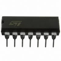
HCF4093BEY STMicroelectronics, HCF4093BEY Datasheet - Page 4

HCF4093BEY
Manufacturer Part Number
HCF4093BEY
Description
IC TRIGGER NAND QUAD 2INP 14-DIP
Manufacturer
STMicroelectronics
Series
4000Br
Specifications of HCF4093BEY
Logic Type
NAND Gate
Number Of Inputs
2
Number Of Circuits
4
Current - Output High, Low
6.8mA, 6.8mA
Voltage - Supply
3 V ~ 20 V
Operating Temperature
-55°C ~ 125°C
Mounting Type
Through Hole
Package / Case
14-DIP (0.300", 7.62mm)
Product
NAND
Logic Family
HCF40
High Level Output Current
- 2.4 mA
Low Level Output Current
2.4 mA
Propagation Delay Time
380 ns
Supply Voltage (max)
20 V
Supply Voltage (min)
3 V
Maximum Operating Temperature
+ 125 C
Mounting Style
Through Hole
Minimum Operating Temperature
- 55 C
Capacitance, Input
5 pF (Typ.) @ 25 °C
Circuit Type
Monolithic Integrated
Current, Input, Leakage
30 to 600 μA (Max.) (Quiescent)
Current, Supply
600 μA
Function Type
2-Inputs
Logic Function
NAND Gate
Package Type
DIP-14
Power Dissipation
200 mW
Special Features
Schmitt-Trigger
Temperature, Operating, Maximum
125 °C
Temperature, Operating, Minimum
-55 °C
Temperature, Operating, Range
-55 to +125 °C
Time, Delay, Propagation
190 ns (Typ.)
Voltage, Supply
3 to 20 V
Lead Free Status / RoHS Status
Contains lead / RoHS non-compliant
Other names
497-1372-5
Available stocks
Company
Part Number
Manufacturer
Quantity
Price
Company:
Part Number:
HCF4093BEY
Manufacturer:
AD
Quantity:
4 300
Part Number:
HCF4093BEY
Manufacturer:
ST
Quantity:
20 000
Maximum ratings
2
2.1
4/13
Maximum ratings
Stressing the device above the rating listed in the “Absolute Maximum Ratings” table may
cause permanent damage to the device. These are stress ratings only and operation of the
device at these or any other conditions above those indicated in the Operating sections of
this specification is not implied. Exposure to Absolute Maximum Rating conditions for
extended periods may affect device reliability. Refer also to the STMicroelectronics SURE
Program and other relevant quality documents.
Table 4.
Recommended operating conditions
Table 5.
Symbol
V
T
T
P
V
DD
I
stg
op
Symbol
I
D
I
V
T
V
DD
op
I
Supply voltage
DC Input voltage
DC Input current
Power dissipation per package
Power dissipation per output transistor
Operating temperature
Storage temperature
Absolute maximum ratings
Recommended operating conditions
Supply voltage
Input voltage
Operating temperature
Parameter
Parameter
-0.5 to V
-0.5 to + 22
-55 to +125
-65 to +150
-55 to 125
Value
0 to V
± 10
200
100
3 to 20
Value
DD
+ 0.5
DD
HCF4093
Unit
mW
mW
mA
Unit
°C
°C
V
V
°C
V
V


