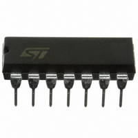
HCF4093BEY STMicroelectronics, HCF4093BEY Datasheet

HCF4093BEY
Specifications of HCF4093BEY
Available stocks
Related parts for HCF4093BEY
HCF4093BEY Summary of contents
Page 1
... Meets all requirements of JEDEC JESD13B "Standard Specifications for Description of B Series CMOS Devices" Table 1. Device summary Order code HCF4093BEY HCF4093M013TR August 2007 QUAD 2-input NAND Schmidt trigger = typ.) DD Description The HCF4093 is a monolithic integrated circuit fabricated in metal oxide semiconductor = 25° ...
Page 2
Pin settings 1 Pin settings 1.1 Pin connection Figure 1. HCF4093B pin connection Figure 2. Input equivalent circuit Table 2. Pin description Pin number 12 10 2/13 Symbol ...
Page 3
HCF4093 Table 3. Truth table Inputs Pin settings Outputs 3/13 ...
Page 4
... These are stress ratings only and operation of the device at these or any other conditions above those indicated in the Operating sections of this specification is not implied. Exposure to Absolute Maximum Rating conditions for extended periods may affect device reliability. Refer also to the STMicroelectronics SURE Program and other relevant quality documents. Table 4. ...
Page 5
HCF4093 3 Electrical characteristics Table 6. DC specification Test Condition Symbol Parameter V I (V) 0/5 0/10 Quiescent I L current 0/15 0/20 0/5 High level V output 0/10 OH voltage 0/15 5/0 Low level V output 10/0 OL voltage ...
Page 6
Electrical characteristics Table 6. DC specification (continued) Test Condition Symbol Parameter V I (V) 0/5 0/5 Output drive I OH current 0/10 0/15 0/5 Output sink I 0/10 OL current 0/15 Input leakage I 0/18 I current Input C I ...
Page 7
HCF4093 3.1 Dynamic electrical characteristics ) Table 7. Dynamic electrical characteristics ( Symbol t t PLH PHL t t TLH THL (*) Typical temperature coefficient for all V Figure 3. Test circuit ...
Page 8
Electrical characteristics Figure 4. Waveform: propagation delay times 8/ MHz; 50% duty cycle) HCF4093 ...
Page 9
HCF4093 4 Package mechanical data In order to meet environmental requirements, ST offers these devices in ECOPACK® packages. These packages have a Lead-free second level interconnect. The category of second level interconnect is marked on the package and on the ...
Page 10
Package mechanical data Figure 6. SO-14 package outline 1. Drawing not to scale. Table 9. SO-14 mechanical data Symbol 10/13 millimeters Min Typ Max ...
Page 11
HCF4093 Figure 7. SO-14 tape and reel information 1. Drawing not to scale. Table 10. SO-14 tape and reel information Symbol millimeters Min Typ Max 330 12.8 13.2 20.2 60 ...
Page 12
Revision history 5 Revision history Table 11. Document revision history Date Sept-2001 16-Aug-2007 12/13 Revision 1 First release Document converted to new ST template, added 2 tape and reel information on page 11 andTable 10: SO-14 tape and reel information ...
Page 13
... HCF4093 Information in this document is provided solely in connection with ST products. STMicroelectronics NV and its subsidiaries (“ST”) reserve the right to make changes, corrections, modifications or improvements, to this document, and the products and services described herein at any time, without notice. All ST products are sold pursuant to ST’s terms and conditions of sale. ...


