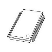
74LVT16374ADGG,112 NXP Semiconductors, 74LVT16374ADGG,112 Datasheet - Page 8

74LVT16374ADGG,112
Manufacturer Part Number
74LVT16374ADGG,112
Description
IC 16BIT EDG-TRIG D FF 48TSSOP
Manufacturer
NXP Semiconductors
Series
74LVTr
Type
D-Type Busr
Specifications of 74LVT16374ADGG,112
Function
Standard
Output Type
Tri-State Non Inverted
Number Of Elements
2
Number Of Bits Per Element
8
Frequency - Clock
150MHz
Delay Time - Propagation
3ns
Trigger Type
Positive Edge
Current - Output High, Low
32mA, 64mA
Voltage - Supply
2.7 V ~ 3.6 V
Operating Temperature
-40°C ~ 85°C
Mounting Type
Surface Mount
Package / Case
48-TSSOP
Logic Family
LVT
Technology
BiCMOS
Number Of Bits
16
Number Of Elements
2
Clock-edge Trigger Type
Positive-Edge
Polarity
Non-Inverting
Operating Supply Voltage (typ)
3.3V
Propagation Delay Time
6ns
Low Level Output Current
64mA
High Level Output Current
-32mA
Operating Supply Voltage (min)
2.7V
Operating Supply Voltage (max)
3.6V
Operating Temp Range
-40C to 85C
Operating Temperature Classification
Industrial
Mounting
Surface Mount
Pin Count
48
Lead Free Status / RoHS Status
Lead free / RoHS Compliant
Other names
935203010112
NXP Semiconductors
Table 6.
At recommended operating conditions; voltages are referenced to GND (ground = 0 V).
[1]
[2]
[3]
[4]
[5]
[6]
[7]
10. Dynamic characteristics
Table 7.
Voltages are referenced to GND (ground = 0 V); for test circuit see
74LVT_LVTH16374A_7
Product data sheet
Symbol Parameter
ΔI
C
C
Symbol
T
f
t
t
t
t
t
t
max
PLH
PHL
PZH
PZL
PHZ
PLZ
amb
I
O
CC
Typical values are measured at V
For valid test results, data must not be loaded into the flips-flops (or latches) after applying power.
Unused pins at V
This is the bus hold overdrive current required to force the input to the opposite logic state.
This parameter is valid for any V
a transition time of 100 μs is permitted. This parameter is valid for T
I
This is the increase in supply current for each input at the specified voltage level other than V
CC
= −40 °C to +85 °C
is measured with outputs pulled to V
additional supply current
input capacitance
output capacitance
Static characteristics
Dynamic characteristics
Parameter
maximum frequency nCP; V
LOW to HIGH
propagation delay
HIGH to LOW
propagation delay
OFF-state to HIGH
propagation delay
OFF-state to LOW
propagation delay
HIGH to OFF-state
propagation delay
LOW to OFF-state
propagation delay
CC
or GND.
CC
CC
Conditions
nCP to nQn; see
nCP to nQn; see
nOE to nQn; see
nOE to nQn; see
nOE to nQn; see
nOE to nQn; see
…continued
between 0 V and 1.2 V with a transition time of up to 10 ms. From V
= 3.3 V and at T
V
V
V
V
V
V
V
V
V
V
V
V
Conditions
per input pin; V
at V
input pins; V
output pins nQn; outputs disabled;
V
CC
CC
CC
CC
CC
CC
CC
CC
CC
CC
CC
CC
O
CC
= 0 V or V
= 3.3 V ± 0.3 V
= 2.7 V
= 3.3 V ± 0.3 V
= 2.7 V
= 3.3 V ± 0.3 V
= 2.7 V
= 3.3 V ± 0.3 V
= 2.7 V
= 3.3 V ± 0.3 V
= 2.7 V
= 3.3 V ± 0.3 V
= 2.7 V
CC
CC
All information provided in this document is subject to legal disclaimers.
or GND.
− 0.6 V, other inputs at V
= 3.3 V ± 0.3 V; see
Rev. 07 — 22 March 2010
I
amb
CC
= 0 V or 3.0 V
Figure 7
Figure 7
Figure 8
Figure 8
Figure 8
Figure 8
CC
74LVT16374A; 74LVTH16374A
= 25 °C.
= 3.0 V to 3.6 V; one input
amb
3.3 V 16-bit edge-triggered D-type flip-flop; 3-state
Figure 7
Figure
= 25 °C only.
CC
or GND
10.
[7]
Min
150
1.5
-
1.5
-
1.5
-
1.5
-
1.5
-
1.5
-
CC
Min
-
-
-
or GND.
CC
Typ
-
2.9
-
3.0
-
3.2
-
3.0
-
3.9
-
3.4
-
= 1.2 V to V
Typ
0.1
3
9
[1]
[1]
© NXP B.V. 2010. All rights reserved.
Max
-
5.0
5.6
5.0
5.6
4.8
6.0
4.6
5.2
5.4
6.0
4.6
5.0
CC
Max
0.2
-
-
= 3.3 V ± 0.3 V
Unit
MHz
ns
ns
ns
ns
ns
ns
ns
ns
ns
ns
ns
ns
Unit
mA
pF
pF
8 of 19


