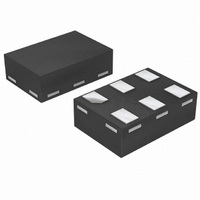
74AUP1G374GF,132 NXP Semiconductors, 74AUP1G374GF,132 Datasheet - Page 3

74AUP1G374GF,132
Manufacturer Part Number
74AUP1G374GF,132
Description
IC F-F D-TYPE POS EDGE 6-XSON
Manufacturer
NXP Semiconductors
Series
74AUPr
Type
D-Typer
Datasheet
1.74AUP1G374GM115.pdf
(23 pages)
Specifications of 74AUP1G374GF,132
Output Type
Tri-State Non Inverted
Package / Case
6-XSON, SOT891
Function
Standard
Number Of Elements
1
Number Of Bits Per Element
1
Frequency - Clock
53MHz
Delay Time - Propagation
23.6ns
Trigger Type
Positive Edge
Current - Output High, Low
4mA, 4mA
Voltage - Supply
0.8 V ~ 3.6 V
Operating Temperature
-40°C ~ 125°C
Mounting Type
Surface Mount
Number Of Circuits
1
Logic Family
AUP
Logic Type
CMOS
Polarity
Non-Inverting
Input Type
Single-Ended
Propagation Delay Time
20.5 ns
High Level Output Current
- 4 mA
Low Level Output Current
4 mA
Supply Voltage (max)
3.6 V
Maximum Operating Temperature
+ 125 C
Mounting Style
SMD/SMT
Minimum Operating Temperature
- 40 C
Supply Voltage (min)
0.8 V
Lead Free Status / RoHS Status
Lead free / RoHS Compliant
Lead Free Status / RoHS Status
Lead free / RoHS Compliant, Lead free / RoHS Compliant
Other names
74AUP1G374GF-H
74AUP1G374GF-H
935281333132
74AUP1G374GF-H
935281333132
NXP Semiconductors
6. Pinning information
Table 3.
7. Functional description
Table 4.
[1]
74AUP1G374
Product data sheet
Symbol
CP
GND
D
Q
V
OE
Operating mode
Load and read register
Load register and disable output
Fig 4.
CC
H = HIGH voltage level;
h = HIGH voltage level one set-up time prior to the HIGH-to-LOW LE transition;
L = LOW voltage level;
l = LOW voltage level one set-up time prior to the HIGH-to-LOW LE transition;
Z = high-impedance OFF-state;
= LOW-to-HIGH clock transition.
GND
CP
D
Pin configuration SOT363
Pin description
Function table
1
2
3
74AUP1G374
6.1 Pinning
6.2 Pin description
001aae460
[1]
6
5
4
Pin
1
2
3
4
5
6
OE
V
Q
CC
All information provided in this document is subject to legal disclaimers.
Fig 5.
Input
OE
L
L
H
H
GND
Description
clock input (LOW-to-HIGH, edge-triggered)
ground (0 V)
data input
3-state flip-flop output
supply voltage
output enable input (active LOW)
Rev. 5 — 14 July 2010
CP
Pin configuration SOT886
D
Transparent top view
74AUP1G374
Low-power D-type flip-flop; positive-edge trigger; 3-state
1
2
3
CP
001aae461
6
5
4
OE
V
Q
CC
D
l
h
l
h
Fig 6.
Internal
flip-flop
L
H
L
H
GND
74AUP1G374
CP
Pin configuration SOT891,
SOT1115 and SOT1202
D
Transparent top view
74AUP1G374
1
2
3
© NXP B.V. 2010. All rights reserved.
001aae462
6
5
4
Output
Q
L
H
Z
Z
OE
V
Q
CC
3 of 23


