74AHC574BQ,115 NXP Semiconductors, 74AHC574BQ,115 Datasheet - Page 5
74AHC574BQ,115
Manufacturer Part Number
74AHC574BQ,115
Description
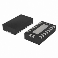
IC OCT D FF POS-EDGTRIG 20DHVQFN
Manufacturer
NXP Semiconductors
Series
74AHCr
Type
D-Type Busr
Datasheet
1.74AHC574PW118.pdf
(18 pages)
Specifications of 74AHC574BQ,115
Function
Standard
Output Type
Tri-State Non Inverted
Number Of Elements
1
Number Of Bits Per Element
8
Frequency - Clock
75MHz
Delay Time - Propagation
9ns
Trigger Type
Positive Edge
Current - Output High, Low
8mA, 8mA
Voltage - Supply
2 V ~ 5.5 V
Operating Temperature
-40°C ~ 125°C
Mounting Type
Surface Mount
Package / Case
20-VQFN Exposed Pad, 20-HVQFN, 20-SQFN, 20-DHVQFN
Number Of Circuits
8
Logic Family
74AHC
Logic Type
CMOS
Polarity
Non-Inverting
Input Type
Single-Ended
Propagation Delay Time
16.7 ns
High Level Output Current
- 8 mA
Supply Voltage (max)
5.5 V
Maximum Operating Temperature
+ 85 C
Mounting Style
SMD/SMT
Minimum Operating Temperature
- 40 C
Supply Voltage (min)
2 V
Lead Free Status / RoHS Status
Lead free / RoHS Compliant
Lead Free Status / RoHS Status
Lead free / RoHS Compliant, Lead free / RoHS Compliant
Other names
74AHC574BQ-G
74AHC574BQ-G
935285546115
74AHC574BQ-G
935285546115
Available stocks
Company
Part Number
Manufacturer
Quantity
Price
Company:

Part Number:
74AHC574BQ,115
Manufacturer:
ROHM
Quantity:
12 000
Company:
Part Number:
74AHC574BQ,115
Manufacturer:
NXP
Quantity:
12 000


NXP Semiconductors
6. Functional description
Table 3.
[1]
7. Limiting values
Table 4.
In accordance with the Absolute Maximum Rating System (IEC 60134). Voltages are referenced to GND (ground = 0 V).
[1]
[2]
[3]
[4]
74AHC_AHCT574_2
Product data sheet
Operating mode
Load and read register
Load register and disable output
Symbol
V
V
I
I
I
I
I
T
P
IK
OK
O
CC
GND
stg
CC
I
tot
H = HIGH voltage level;
h = HIGH voltage level one setup time prior to the HIGH-to-LOW CP transition;
L = LOW voltage level;
l = LOW voltage level one setup time prior to the HIGH-to-LOW CP transition;
Z = high-impedance OFF-state;
The input and output voltage ratings may be exceeded if the input and output current ratings are observed.
P
P
P
tot
tot
tot
= LOW-to-HIGH clock transition.
derates linearly with 8 mW/K above 70 C.
derates linearly with 5.5 mW/K above 60 C.
derates linearly with 4.5 mW/K above 60 C.
Function table
Limiting values
Parameter
supply voltage
input voltage
input clamping current
output clamping current
output current
supply current
ground current
storage temperature
total power dissipation
SO20 package
TSSOP20 package
DHVQFN20 package
[1]
Input
OE
L
L
H
H
Conditions
V
V
V
T
Rev. 02 — 24 January 2008
amb
I
O
O
< 0.5 V
< 0.5 V or V
= 0.5 V to (V
= 40 C to +125 C
CP
Octal D-type flip-flop; positive edge-trigger; 3-state
O
CC
> V
74AHC574; 74AHCT574
+ 0.5 V)
CC
+ 0.5 V
Dn
l
h
l
h
Internal
flip-flop
L
H
L
H
[1]
[1]
[2]
[3]
[4]
Min
-
-
-
-
-
-
0.5
0.5
20
75
65
© NXP B.V. 2008. All rights reserved.
Max
+7.0
+7.0
-
75
-
+150
500
500
500
20
25
Output
Qn
L
H
Z
Z
Unit
V
V
mA
mA
mA
mA
mA
mW
mW
mW
C
5 of 18
Related parts for 74AHC574BQ,115
Image
Part Number
Description
Manufacturer
Datasheet
Request
R

Part Number:
Description:
Octal D-type ?ip-?op; Positive Edge-trigger; 3-state
Manufacturer:
NXP Semiconductors
Datasheet:
Part Number:
Description:
NXP Semiconductors designed the LPC2420/2460 microcontroller around a 16-bit/32-bitARM7TDMI-S CPU core with real-time debug interfaces that include both JTAG andembedded trace
Manufacturer:
NXP Semiconductors
Datasheet:

Part Number:
Description:
NXP Semiconductors designed the LPC2458 microcontroller around a 16-bit/32-bitARM7TDMI-S CPU core with real-time debug interfaces that include both JTAG andembedded trace
Manufacturer:
NXP Semiconductors
Datasheet:
Part Number:
Description:
NXP Semiconductors designed the LPC2468 microcontroller around a 16-bit/32-bitARM7TDMI-S CPU core with real-time debug interfaces that include both JTAG andembedded trace
Manufacturer:
NXP Semiconductors
Datasheet:
Part Number:
Description:
NXP Semiconductors designed the LPC2470 microcontroller, powered by theARM7TDMI-S core, to be a highly integrated microcontroller for a wide range ofapplications that require advanced communications and high quality graphic displays
Manufacturer:
NXP Semiconductors
Datasheet:
Part Number:
Description:
NXP Semiconductors designed the LPC2478 microcontroller, powered by theARM7TDMI-S core, to be a highly integrated microcontroller for a wide range ofapplications that require advanced communications and high quality graphic displays
Manufacturer:
NXP Semiconductors
Datasheet:
Part Number:
Description:
The Philips Semiconductors XA (eXtended Architecture) family of 16-bit single-chip microcontrollers is powerful enough to easily handle the requirements of high performance embedded applications, yet inexpensive enough to compete in the market for hi
Manufacturer:
NXP Semiconductors
Datasheet:
Part Number:
Description:
The XA-S3 device is a member of Philips Semiconductors? XA(eXtended Architecture) family of high performance 16-bitsingle-chip microcontrollers
Manufacturer:
NXP Semiconductors
Datasheet:

Part Number:
Description:
The NXP BlueStreak LH75401/LH75411 family consists of two low-cost 16/32-bit System-on-Chip (SoC) devices
Manufacturer:
NXP Semiconductors
Datasheet:
Part Number:
Description:
The NXP LPC3130/3131 combine an 180 MHz ARM926EJ-S CPU core, high-speed USB2
Manufacturer:
NXP Semiconductors
Datasheet:
Part Number:
Description:
The NXP LPC3141 combine a 270 MHz ARM926EJ-S CPU core, High-speed USB 2
Manufacturer:
NXP Semiconductors
Part Number:
Description:
The NXP LPC3143 combine a 270 MHz ARM926EJ-S CPU core, High-speed USB 2
Manufacturer:
NXP Semiconductors

Part Number:
Description:
The NXP LPC3152 combines an 180 MHz ARM926EJ-S CPU core, High-speed USB 2
Manufacturer:
NXP Semiconductors
Part Number:
Description:
The NXP LPC3154 combines an 180 MHz ARM926EJ-S CPU core, High-speed USB 2
Manufacturer:
NXP Semiconductors