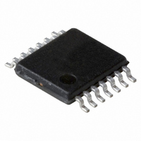
74LV74PW,118 NXP Semiconductors, 74LV74PW,118 Datasheet - Page 6

74LV74PW,118
Manufacturer Part Number
74LV74PW,118
Description
IC DUAL D FF POSEDG TRIG 14TSSOP
Manufacturer
NXP Semiconductors
Series
74LVr
Type
D-Typer
Specifications of 74LV74PW,118
Output Type
Differential
Package / Case
14-TSSOP
Function
Set(Preset) and Reset
Number Of Elements
2
Number Of Bits Per Element
1
Frequency - Clock
56MHz
Trigger Type
Positive Edge
Current - Output High, Low
12mA, 12mA
Voltage - Supply
1 V ~ 5.5 V
Operating Temperature
-40°C ~ 125°C
Mounting Type
Surface Mount
Number Of Circuits
2
Logic Family
LV
Logic Type
D-Type Edge Triggered Flip-Flop
Polarity
Inverting/Non-Inverting
Input Type
Single-Ended
Propagation Delay Time
11 ns at 3.3 V
High Level Output Current
- 12 mA
Low Level Output Current
12 mA
Supply Voltage (max)
5.5 V
Maximum Operating Temperature
+ 125 C
Mounting Style
SMD/SMT
Minimum Operating Temperature
- 40 C
Supply Voltage (min)
1 V
Delay Time - Propagation
-
Technology
CMOS
Number Of Bits
2
Number Of Elements
2
Clock-edge Trigger Type
Positive-Edge
Operating Supply Voltage (typ)
3.3V
Package Type
TSSOP
Frequency (max)
56MHz
Operating Supply Voltage (min)
1V
Operating Supply Voltage (max)
5.5V
Operating Temp Range
-40C to 125C
Operating Temperature Classification
Automotive
Mounting
Surface Mount
Pin Count
14
Lead Free Status / RoHS Status
Lead free / RoHS Compliant
Delay Time - Propagation
-
Lead Free Status / Rohs Status
Lead free / RoHS Compliant
Other names
74LV74PW-T
74LV74PW-T
935175140118
74LV74PW-T
935175140118
1. Unless otherwise stated, all typical values are at T
2. Typical value measured at V
3. Typical value measured at V
Philips Semiconductors
AC CHARACTERISTICS
GND = 0V; t
NOTE:
1998 Apr 20
SYMBOL
t
t
t
PHL/
PHL/
PHL/
Dual D-type flip-flop with set and reset;
positive edge-trigger
f
f
t
max
rem
t
t
t
t
t
su
t
W
W
W
W
h
t
t
t
PLH
PLH
PLH
r
= t
Propagation delay
Propagation delay
nCP to nQ, nQ
nCP to nQ, nQ
Propagation delay
Propagation delay
nS
nS
Propagation delay
Propagation delay
nR
nR
Clock pulse width
HIGH to LOW
Set or reset pulse
width LOW
Removal time
Removal time
set or reset
set or reset
Set up time
Set-up time
nD to nCP
nD to nCP
Hold time
Hold time
nD to nCP
nD to nCP
Maximum clock
pulse frequency
f
v 2.5ns; C
D
D
PARAMETER
D
D
to nQ, nQ
to nQ, nQ
to nQ, nQ
to nQ, nQ
L
= 50pF; R
CC
CC
= 3.3V.
= 5.0V.
WAVEFORM
Figures, 1, 3
Figures 2, 3
Figures 2, 3
L
Figure 1
Figure 1
Figure 2
Figure 2
Figure 2
Figure 1
Figure 1
Figure 1
Figure 1
= 1K
amb
= 25 C.
CONDITION
3.0 to 3.6
4.5 to 5.5
3.0 to 3.6
4.5 to 5.5
3.0 to 3.6
4.5 to 5.5
3.0 to 3.6
4.5 to 5.5
3.0 to 3.6
4.5 to 5.5
3.0 to 3.6
4.5 to 5.5
3.0 to 3.6
4.5 to 5.5
3.0 to 3.6
4.5 to 5.5
3.0 to 3.6
4.5 to 5.5
V
CC
1.2
2.0
2.7
1.2
2.0
2.7
1.2
2.0
2.7
2.0
2.7
2.0
2.7
1.2
2.0
2.7
1.2
2.0
2.7
1.2
2.0
2.7
2.0
2.7
(V)
6
MIN
34
25
20
15
34
25
20
15
14
10
22
12
14
50
60
70
–
–
–
–
–
–
–
–
–
–
–
–
–
–
–
–
8
6
–
8
6
–
3
3
3
3
–40 to +85 C
LIMITS
TYP
100
110
9.5
–10
13
17
12
17
12
–2
–2
70
24
18
90
31
23
90
31
23
10
7
6
10
7
6
1
1
10
2
1
–2
–2
40
90
8
8
5
2
1
4
3
2
3
2
3
2
3
2
2
2
2
3
2
3
2
3
3
3
2
1
MAX
44
28
26
17
46
34
27
19
46
34
27
19
–
–
–
–
–
–
–
–
–
–
–
–
–
–
–
–
–
–
–
–
–
–
–
–
–
–
–
–
–
–
–40 to +125 C
MIN
41
30
24
18
41
30
24
18
15
11
26
15
10
12
40
48
56
–
–
–
–
–
–
–
–
–
–
–
–
–
–
–
–
9
7
–
8
–
3
3
3
3
LIMITS
Product specification
MAX
56
41
33
23
58
43
34
24
58
43
34
24
–
–
–
–
–
–
–
–
–
–
–
–
–
–
–
–
–
–
–
–
–
–
–
–
–
–
–
–
–
–
74LV74
UNIT
MHz
MHz
ns
ns
ns
ns
ns
ns
ns
ns
ns
ns


