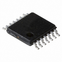
74LV74PW,118 NXP Semiconductors, 74LV74PW,118 Datasheet - Page 4

74LV74PW,118
Manufacturer Part Number
74LV74PW,118
Description
IC DUAL D FF POSEDG TRIG 14TSSOP
Manufacturer
NXP Semiconductors
Series
74LVr
Type
D-Typer
Specifications of 74LV74PW,118
Output Type
Differential
Package / Case
14-TSSOP
Function
Set(Preset) and Reset
Number Of Elements
2
Number Of Bits Per Element
1
Frequency - Clock
56MHz
Trigger Type
Positive Edge
Current - Output High, Low
12mA, 12mA
Voltage - Supply
1 V ~ 5.5 V
Operating Temperature
-40°C ~ 125°C
Mounting Type
Surface Mount
Number Of Circuits
2
Logic Family
LV
Logic Type
D-Type Edge Triggered Flip-Flop
Polarity
Inverting/Non-Inverting
Input Type
Single-Ended
Propagation Delay Time
11 ns at 3.3 V
High Level Output Current
- 12 mA
Low Level Output Current
12 mA
Supply Voltage (max)
5.5 V
Maximum Operating Temperature
+ 125 C
Mounting Style
SMD/SMT
Minimum Operating Temperature
- 40 C
Supply Voltage (min)
1 V
Delay Time - Propagation
-
Technology
CMOS
Number Of Bits
2
Number Of Elements
2
Clock-edge Trigger Type
Positive-Edge
Operating Supply Voltage (typ)
3.3V
Package Type
TSSOP
Frequency (max)
56MHz
Operating Supply Voltage (min)
1V
Operating Supply Voltage (max)
5.5V
Operating Temp Range
-40C to 125C
Operating Temperature Classification
Automotive
Mounting
Surface Mount
Pin Count
14
Lead Free Status / RoHS Status
Lead free / RoHS Compliant
Delay Time - Propagation
-
Lead Free Status / Rohs Status
Lead free / RoHS Compliant
Other names
74LV74PW-T
74LV74PW-T
935175140118
74LV74PW-T
935175140118
1. The LV is guaranteed to function down to V
1. Stresses beyond those listed may cause permanent damage to the device. These are stress ratings only and functional operation of the
2. The input and output voltage ratings may be exceeded if the input and output current ratings are observed.
Philips Semiconductors
LOGIC DIAGRAM (ONE FLIP-FLOP)
RECOMMENDED OPERATING CONDITIONS
NOTE:
ABSOLUTE MAXIMUM RATINGS
In accordance with the Absolute Maximum Rating System (IEC 134)
Voltages are referenced to GND (ground = 0V)
NOTES:
1998 Apr 20
SYMBOL
SYMBOL
Dual D-type flip-flop with set and reset;
positive edge-trigger
device at these or any other conditions beyond those indicated under “recommended operating conditions” is not implied. Exposure to
absolute-maximum-rated conditions for extended periods may affect device reliability.
T
V
I
V
T
P
P
t
GND
V
I
I
amb
r
V
stg
CC
I
CC
, t
OK
I
CC
t t
tot
IK
O
O
I
f
,
DC supply voltage
DC input diode current
DC output diode current
DC output source or sink current
– standard outputs
DC V
–standard outputs
Storage temperature range
Power dissipation per package
–plastic DIL
–plastic mini-pack (SO)
–plastic shrink mini-pack (SSOP and TSSOP)
DC supply voltage
Input voltage
Output voltage
Operating ambient temperature range in free
air
Input rise and fall times except for
Schmitt-trigger inputs
CC
or GND current for types with
CP
R
S
D
D
D
PARAMETER
PARAMETER
1, 2
CC
= 1.0V (input levels GND or V
C
C
C
C
C
C
See DC and AC
characteristics
V
V
–0.5V < V
for temperature range: –40 to +125 C
above +70 C derate linearly with 12mW/K
above +70 C derate linearly with 8 mW/K
above +60 C derate linearly with 5.5 mW/K
I
O
< –0.5 or V
V
V
V
V
< –0.5 or V
CC
CC
CC
CC
CONDITIONS
4
See Note1
= 1.0V to 2.0V
= 2.0V to 2.7V
= 2.7V to 3.6V
= 3.6V to 5.5V
O
CC
< V
); DC characteristics are guaranteed from V
I
O
> V
CONDITIONS
CC
> V
CC
+ 0.5V
CC
+ 0.5V
C
C
+ 0.5V
MIN
–40
–40
1.0
0
0
–
–
–
–
C
C
TYP.
3.3
–
–
–
–
–
–
–0.5 to +7.0
–65 to +150
RATING
750
500
400
CC
20
50
25
50
+125
MAX
V
V
+85
500
200
100
5.5
50
CC
CC
= 1.2V to V
Product specification
SV00334
74LV74
Q
Q
UNIT
CC
ns/V
UNIT
mW
mW
V
V
V
mA
mA
mA
mA
C
V
= 5.5V.
C


