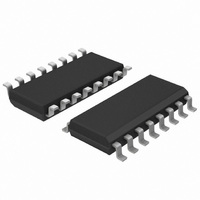
74HCT40105D,112 NXP Semiconductors, 74HCT40105D,112 Datasheet - Page 14

74HCT40105D,112
Manufacturer Part Number
74HCT40105D,112
Description
IC 4X16 FIFO REGISTER 16-SOIC
Manufacturer
NXP Semiconductors
Series
74HCTr
Specifications of 74HCT40105D,112
Package / Case
16-SOIC (3.9mm Width)
Function
Asynchronous
Memory Size
64 (4 x 16)
Data Rate
25MHz
Voltage - Supply
4.5 V ~ 5.5 V
Mounting Type
Surface Mount
Logic Family
HCT
Number Of Circuits
1
Maximum Clock Frequency
36 MHz
High Level Output Current
- 6 mA
Low Level Output Current
6 mA
Supply Voltage (max)
5.5 V
Maximum Operating Temperature
+ 125 C
Minimum Operating Temperature
- 40 C
Mounting Style
SMD/SMT
Supply Voltage (min)
4.5 V
Logic Type
CMOS
Lead Free Status / RoHS Status
Lead free / RoHS Compliant
Operating Temperature
-
Access Time
-
Lead Free Status / Rohs Status
Lead free / RoHS Compliant
Other names
568-2839-5
933715220112
933715220112
Philips Semiconductors
Shift-out operation; high-speed burst mode
1998 Jan 23
4-bit x 16-word FIFO register
In the high-speed mode, the burst-out rate is determined by the
minimum shift-out HIGH and shift-out LOW specifications. The
DOR flag is a don’t care condition and a SO pulse can be applied
without regard to the flag.
(1) HC : V
Fig.12 Waveforms showing SO minimum pulse width and maximum pulse frequency, in high-speed shift-out
The shaded areas indicate when the input is permitted
to change for predictable output performance.
(1) HC : V
(1) HC : V
HCT : V
HCT : V
HCT : V
burst mode.
Fig.14 Waveforms showing SO input to Q
M
M
M
M
M
M
= 50%; V
= 1.3 V; V
= 50%; V
= 1.3 V; V
= 50%; V
= 1.3 V; V
I
I
I
I
I
I
= GND to V
= GND to V
= GND to V
Fig.13 Waveforms showing hold and set up times for D
= GND to 3 V.
= GND to 3 V.
= GND to 3 V.
CC
CC
CC
.
.
.
n
output propagation delays and output transition time.
14
n
input to SI input.
74HC/HCT40105
Product specification


