IDT72V04L25J IDT, Integrated Device Technology Inc, IDT72V04L25J Datasheet - Page 4
IDT72V04L25J
Manufacturer Part Number
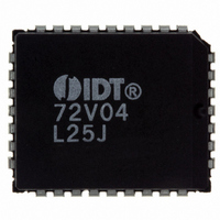
IDT72V04L25J
Description
IC FIFO ASYNCH 4KX9 25NS 32PLCC
Manufacturer
IDT, Integrated Device Technology Inc
Series
72Vr
Datasheet
1.IDT72V04L25J.pdf
(12 pages)
Specifications of IDT72V04L25J
Function
Asynchronous
Memory Size
36K (4K x 9)
Access Time
25ns
Voltage - Supply
3 V ~ 3.6 V
Operating Temperature
0°C ~ 70°C
Mounting Type
Surface Mount
Package / Case
32-PLCC
Lead Free Status / RoHS Status
Contains lead / RoHS non-compliant
Data Rate
-
Other names
72V04L25J
800-1508
800-1508-5
800-1508
800-1508
800-1508-5
800-1508
Available stocks
Company
Part Number
Manufacturer
Quantity
Price
Company:

Part Number:
IDT72V04L25J
Manufacturer:
IDT
Quantity:
3 000
Company:
Part Number:
IDT72V04L25J
Manufacturer:
IDT, Integrated Device Technology Inc
Quantity:
10 000
Company:
Part Number:
IDT72V04L25J8
Manufacturer:
IDT, Integrated Device Technology Inc
Quantity:
10 000
Company:
Part Number:
IDT72V04L25JGI
Manufacturer:
IDT
Quantity:
1 238
Company:
Part Number:
IDT72V04L25JGI
Manufacturer:
IDT, Integrated Device Technology Inc
Quantity:
10 000
Company:
Part Number:
IDT72V04L25JGI8
Manufacturer:
IDT, Integrated Device Technology Inc
Quantity:
10 000
Company:
Part Number:
IDT72V04L25JI
Manufacturer:
IDT
Quantity:
3 000
Company:
Part Number:
IDT72V04L25JI
Manufacturer:
IDT
Quantity:
17
Company:
Part Number:
IDT72V04L25JI
Manufacturer:
IDT, Integrated Device Technology Inc
Quantity:
10 000


SIGNAL DESCRIPTIONS
INPUTS:
DATA IN (D
CONTROLS:
RESET (RS)
state. During reset, both internal read and write pointers are set to the first
location. A reset is required after power up before a write operation can take
place. Both the Read Enable (R) and Write Enable (W) inputs must be
in the HIGH state during the window shown in Figure 2, (i.e., t
before the rising edge of RS ) and should not change until t
the rising edge of RS. Half-Full Flag (HF) will be reset to HIGH after
Reset (RS).
WRITE ENABLE (W)
is not set. Data setup and hold times must be adhered to with respect to the rising
edge of the Write Enable (W). Data is stored in the RAM array sequentially and
independently of any ongoing read operation.
operation, the Half-Full Flag (HF) will be set to LOW and will remain set until the
difference between the write pointer and read pointer is less than or equal to
one half of the total memory of the device. The Half-Full Flag (HF) is then reset
by the rising edge of the read operation.
write operations. Upon the completion of a valid read operation, the Full Flag
(FF) will go HIGH after t
is full, the internal write pointer is blocked from W, so external changes in W will
not affect the FIFO when it is full.
READ ENABLE (R)
the Empty Flag (EF) is not set. The data is accessed on a First-In/First-Out basis,
independent of any ongoing write operations. After Read Enable (R) goes
HIGH, the Data Outputs (Q
the next Read operation. When all data has been read from the FIFO, the Empty
Flag (EF) will go LOW, allowing the “final” read cycle but inhibiting further read
operations with the data outputs remaining in a high impedance state. Once a
valid write operation has been accomplished, the Empty Flag (EF) will go HIGH
after t
read pointer is blocked from R so external changes in R will not affect the FIFO
when it is empty.
IDT72V01/72V02/72V03/72V04/72V05/72V06 3.3V ASYNCHRONOUS FIFO
512 x 9, 1,024 x 9, 2,048 x 9, 4,096 x 9, 8,192 x 9 and 16,384 x 9
Data inputs for 9-bit wide data.
Reset is accomplished whenever the Reset (RS) input is taken to a LOW
A write cycle is initiated on the falling edge of this input if the Full Flag (FF)
After half of the memory is filled and at the falling edge of the next write
To prevent data overflow, the Full Flag (FF) will go LOW, inhibiting further
A read cycle is initiated on the falling edge of the Read Enable (R) provided
WEF
and a valid Read can then begin. When the FIFO is empty, the internal
0
– D
8
)
RFF
0
– Q
, allowing a valid write to begin. When the FIFO
8
) will return to a high impedance condition until
RSR
after
RSS
4
FIRST LOAD/RETRANSMIT (FL/RT)
grounded to indicate that it is the first loaded (see Operating Modes). In the Single
Device Mode, this pin acts as the retransmit input. The Single Device Mode is
initiated by grounding the Expansion In (XI).
control (RT) input is pulsed LOW. A retransmit operation will set the internal read
pointer to the first location and will not affect the write pointer. Read Enable (R)
and Write Enable (W) must be in the HIGH state during retransmit. This feature
is useful when less than 512/1,024/2,048/4,096/8,192/16,384 writes are
performed between resets. The retransmit feature is not compatible with the
Depth Expansion Mode and will affect the Half-Full Flag (HF), depending on
the relative locations of the read and write pointers.
EXPANSION IN (XI)
an operation in the single device mode. Expansion In (XI) is connected to
Expansion Out (XO) of the previous device in the Depth Expansion or Daisy
Chain Mode.
OUTPUTS:
FULL FLAG (FF)
write pointer is one location less than the read pointer, indicating that the device
is full. If the read pointer is not moved after Reset (RS), the Full-Flag (FF) will
go LOW after 512/1,024/2,048/4,096/8,192/16,384 writes to the IDT72V01/
72V02/72V03/72V04/72V05/72V06.
EMPTY FLAG (EF)
the read pointer is equal to the write pointer, indicating that the device is empty.
EXPANSION OUT/HALF-FULL FLAG (XO/HF)
In (XI) is grounded, this output acts as an indication of a half-full memory.
operation, the Half-Full Flag (HF) will be set LOW and will remain set until the
difference between the write pointer and read pointer is less than or equal to
one half of the total memory of the device. The Half-Full Flag (HF) is then reset
by using rising edge of the read operation.
Out (XO) of the previous device. This output acts as a signal to the next device
in the Daisy Chain by providing a pulse to the next device when the previous
device reaches the last location of memory.
DATA OUTPUTS (Q
whenever Read (R) is in a HIGH state.
This is a dual-purpose input. In the Depth Expansion Mode, this pin is
These FIFOs can be made to retransmit data when the Retransmit Enable
This input is a dual-purpose pin. Expansion In (XI) is grounded to indicate
The Full Flag (FF) will go LOW, inhibiting further write operation, when the
The Empty Flag (EF) will go LOW, inhibiting further read operations, when
This is a dual-purpose output. In the single device mode, when Expansion
After half of the memory is filled and at the falling edge of the next write
In the Depth Expansion Mode, Expansion In (XI) is connected to Expansion
Data outputs for 9-bit wide data. This data is in a high impedance condition
0
– Q
8
)
COMMERCIAL AND INDUSTRIAL
TEMPERATURE RANGES
OCTOBER 22, 2008
Related parts for IDT72V04L25J
Image
Part Number
Description
Manufacturer
Datasheet
Request
R

Part Number:
Description:
TRANSLATION DEVICE DPI 80-PQFP
Manufacturer:
IDT, Integrated Device Technology Inc
Datasheet:
Part Number:
Description:
IDT PART
Manufacturer:
IDT, Integrated Device Technology Inc
Datasheet:
Part Number:
Description:
IC LIU T1/E1/J1 OCTAL 256PBGA
Manufacturer:
IDT, Integrated Device Technology Inc
Datasheet:

Part Number:
Description:
IC FREQ TIMING GENERATOR 28TSSOP
Manufacturer:
IDT, Integrated Device Technology Inc
Datasheet:
Part Number:
Description:
IC CLK DVR PLL 1:10 40VFQFPN
Manufacturer:
IDT, Integrated Device Technology Inc
Datasheet:
Part Number:
Description:
IC CLK FANOUT BUFFER 1:18 32LQFP
Manufacturer:
IDT, Integrated Device Technology Inc
Datasheet:
Part Number:
Description:
IC CLK FANOUT BUFFER 1:18 32LQFP
Manufacturer:
IDT, Integrated Device Technology Inc
Datasheet:
Part Number:
Description:
IC CK505 VREG/RES 56TSSOP
Manufacturer:
IDT, Integrated Device Technology Inc
Datasheet:

Part Number:
Description:
IC SDRAM CLK DVR 1:10 48-TSSOP
Manufacturer:
IDT, Integrated Device Technology Inc
Datasheet:

Part Number:
Description:
IC CLK DVR PLL 1:10 48TSSOP
Manufacturer:
IDT, Integrated Device Technology Inc
Datasheet:
Part Number:
Description:
IC FLEXPC CLK PROGR P4 56-TSSOP
Manufacturer:
IDT, Integrated Device Technology Inc
Datasheet:
Part Number:
Description:
IC FLEXPC CLK PROGR P4 56-TSSOP
Manufacturer:
IDT, Integrated Device Technology Inc
Datasheet:
Part Number:
Description:
IC FLEXPC CLK PROGR P4 56-SSOP
Manufacturer:
IDT, Integrated Device Technology Inc
Datasheet:

Part Number:
Description:
IC PLL CLK DRIVER 2.5V 28-TSSOP
Manufacturer:
IDT, Integrated Device Technology Inc
Datasheet:
Part Number:
Description:
IC CLOCK DRIVER 2.5V 24-TSSOP
Manufacturer:
IDT, Integrated Device Technology Inc
Datasheet: