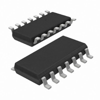
74HC125D,653 NXP Semiconductors, 74HC125D,653 Datasheet - Page 17

74HC125D,653
Manufacturer Part Number
74HC125D,653
Description
IC BUFFER DVR TRI-ST QD 14SOICN
Manufacturer
NXP Semiconductors
Series
74HCr
Datasheets
1.74HCT4046ADB112.pdf
(19 pages)
2.74HCT4046ADB112.pdf
(23 pages)
3.74HCT125D653.pdf
(6 pages)
Specifications of 74HC125D,653
Logic Type
Buffer/Line Driver, Non-Inverting
Package / Case
14-SOIC (3.9mm Width), 14-SOL
Number Of Elements
4
Number Of Bits Per Element
1
Current - Output High, Low
7.8mA, 7.8mA
Voltage - Supply
2 V ~ 6 V
Mounting Type
Surface Mount
Logic Family
74HC
Number Of Channels Per Chip
4
Polarity
Non-Inverting
Supply Voltage (max)
6 V
Supply Voltage (min)
2 V
Maximum Operating Temperature
125 C
Mounting Style
SMD/SMT
High Level Output Current
- 7.8 mA
Input Bias Current (max)
8 uA
Low Level Output Current
7.8 mA
Maximum Power Dissipation
500 mW
Minimum Operating Temperature
- 40 C
Number Of Lines (input / Output)
8 / 4
Output Type
3-State
Propagation Delay Time
9 ns
Lead Free Status / RoHS Status
Lead free / RoHS Compliant
Operating Temperature
-
Lead Free Status / Rohs Status
Lead free / RoHS Compliant
Other names
568-1392-2
74HC125D-T
933756990653
74HC125D-T
933756990653
Available stocks
Company
Part Number
Manufacturer
Quantity
Price
Part Number:
74HC125D,653
Manufacturer:
NXP/恩智浦
Quantity:
20 000
Philips Semiconductors
DEFINITIONS OF SYMBOLS AND TERMS USED IN
HCMOS DATA SHEETS
Currents
Positive current is defined as conventional current flow
into a device.
Negative current is defined as conventional current flow
out of a device.
Voltages
All voltages are referenced to GND (ground), which is
typically 0 V.
March 1988
I
I
I
I
I
I
I
I
GND
V
V
V
V
CC
GND
I
IK
O
OK
OZ
S
I
CC
EE
H
IH
HCMOS family characteristics
CC
Quiescent power supply current; the current
flowing into the V
Additional quiescent supply current per input
pin at a specified input voltage and V
Quiescent power supply current; the current
flowing into the GND terminal.
Input leakage current; the current flowing into a
device at a specified input voltage and V
Input diode current; the current flowing into a
device at a specified input voltage.
Output source or sink current: the current
flowing into a device at a specified output
voltage.
Output diode current; the current flowing into a
device at a specified output voltage.
OFF-state output current; the leakage current
flowing into the output of a 3-state device in the
OFF-state, when the output is connected to
V
Analog switch leakage current; the current
flowing into an analog switch at a specified
voltage across the switch and V
Supply voltage; for a device with a single
negative power supply, the most negative
power supply, used as the reference level for
other voltages; typically ground.
Supply voltage; the most positive potential on
the device.
Supply voltage; one of two (GND and V
negative power supplies.
Hysteresis voltage; difference between the
trigger levels, when applying a positive and a
negative-going input signal.
HIGH level input voltage; the range of input
voltages that represents a logic HIGH level in
the system.
CC
or GND.
CC
supply terminal.
CC
.
CC
.
EE
CC
)
.
17
Analog terms
Capacitances
V
V
V
V
V
R
C
C
C
C
C
IL
OH
OL
T
T
R
ON
I
I/O
L
PD
S
ON
LOW level input voltage; the range of input
voltages that represents a logic LOW level in
the system.
HIGH level output voltage; the range of
voltages at an output terminal with a specified
output loading and supply voltage. Device
inputs are conditioned to establish a HIGH level
at the output.
LOW level output voltage; the range of voltages
at an output terminal with a specified output
loading and supply voltage. Device inputs are
conditioned to establish a LOW level at the
output.
Trigger threshold voltage; positive-going signal.
Trigger threshold voltage; negative-going
signal.
ON-resistance; the effective ON-state
resistance of an analog switch, at a specified
voltage across the switch and output load.
ON-resistance between any two switches of an
analog device at a specified voltage across the
switch and output load.
Input capacitance; the capacitance measured
at a terminal connected to an input of a device.
Input/Output capacitance; the capacitance
measured at a terminal connected to an I/O-pin
(e.g. a transceiver).
Output load capacitance; the capacitance
connected to an output terminal including jig
and probe capacitance.
Power dissipation capacitance; the capacitance
used to determine the dynamic power
dissipation per logic function, when no extra
load is provided to the device.
Switch capacitance; the capacitance of a
terminal to a switch of an analog device.
ON-resistance; the difference in
FAMILY SPECIFICATIONS


