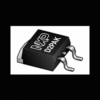
PSMN6R5-80BS NXP Semiconductors, PSMN6R5-80BS Datasheet - Page 2

PSMN6R5-80BS
Manufacturer Part Number
PSMN6R5-80BS
Description
Manufacturer
NXP Semiconductors
Datasheet
1.PSMN6R5-80BS.pdf
(14 pages)
NXP Semiconductors
2. Pinning information
Table 2.
[1]
3. Ordering information
Table 3.
4. Limiting values
Table 4.
In accordance with the Absolute Maximum Rating System (IEC 60134).
[1]
PSMN6R5-80BS
Product data sheet
Pin
1
2
3
mb
Type number
PSMN6R5-80BS
Symbol
V
V
V
I
I
P
T
T
T
Source-drain diode
I
I
Avalanche ruggedness
E
D
DM
S
SM
stg
j
sld(M)
DS
DGR
GS
tot
DS(AL)S
It is not possible to make connection to pin 2.
Continuous current rating is limited by package.
Symbol Description
G
D
S
D
Pinning information
Ordering information
Limiting values
Parameter
drain-source voltage
drain-gate voltage
gate-source voltage
drain current
peak drain current
total power dissipation
storage temperature
junction temperature
peak soldering temperature
source current
peak source current
non-repetitive drain-source
avalanche energy
gate
drain
source
mounting base; connected to
drain
D2PAK
Package
Name
[1]
Description
plastic single-ended surface-mounted package (D2PAK); 3 leads
(one lead cropped)
Conditions
T
T
V
V
pulsed; t
T
T
pulsed; t
V
R
All information provided in this document is subject to legal disclaimers.
j
j
mb
mb
GS
GS
GS
GS
≥ 25 °C; T
≥ 25 °C; T
= 25 °C; see
= 25 °C
= 10 V; T
= 10 V; T
= 10 V; T
= 50 Ω; unclamped
p
p
Rev. 2 — 2 March 2012
Simplified outline
≤ 10 µs; T
≤ 10 µs; T
j
j
≤ 175 °C
≤ 175 °C; R
mb
mb
j(init)
N-channel 80V 6.9mΩ standard level MOSFET in D2PAK
SOT404 (D2PAK)
= 100 °C; see
= 25 °C; see
Figure 2
= 25 °C; I
mb
mb
1
= 25 °C; see
= 25 °C
mb
2
GS
3
D
= 20 kΩ
= 49 A; V
Figure 1
Figure 1
Figure 3
sup
Graphic symbol
≤ 80 V;
PSMN6R5-80BS
[1]
mbb076
G
Min
-
-
-20
-
-
-
-
-55
-55
-
-
-
-
© NXP B.V. 2012. All rights reserved.
D
S
Version
SOT404
Max
80
80
20
82
100
470
210
175
175
260
100
470
700
V
°C
°C
°C
Unit
V
V
A
A
A
W
A
A
mJ
2 of 14


