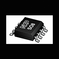
PHKD3NQ10T NXP Semiconductors, PHKD3NQ10T Datasheet - Page 6

PHKD3NQ10T
Manufacturer Part Number
PHKD3NQ10T
Description
Dual standard level N-channel enhancement mode Field-Effect Transistor (FET) in a plastic package using TrenchMOS technology
Manufacturer
NXP Semiconductors
Datasheet
1.PHKD3NQ10T.pdf
(12 pages)
Available stocks
Company
Part Number
Manufacturer
Quantity
Price
Company:
Part Number:
PHKD3NQ10T
Manufacturer:
NXP
Quantity:
36 000
NXP Semiconductors
PHKD3NQ10T
Product data sheet
Fig 5.
Fig 7.
Fig 9.
(A)
(A)
I
I
a
D
D
2.9
2.1
1.3
0.5
6
4
2
0
6
4
2
0
−60
function of drain-source voltage; typical values
function of gate-source voltage; typical values
factor as a function of junction temperature
T
Output characteristics: drain current as a
V
Transfer characteristics: drain current as a
Normalized drain-source on-state resistance
0
0
j
DS
= 25 °C
> I
D
0.4
8
x R
6
DSon
20
2
V
5.4
GS
T
0.8
j
= 150 °C
(V) = 10
1.2
100
4
T
V
1.6
T
j
All information provided in this document is subject to legal disclaimers.
GS
j
= 25 °C
(°C)
5.2
4.8
4.6
4.4
003aaf128
V
003aaf130
003aaf132
5
DS
(V)
(V)
Rev. 02 — 16 December 2010
180
2.0
6
Fig 6.
Fig 8.
Fig 10. Gate-source threshold voltage as a function of
R
V
DS(on)
GS(th)
(Ω)
G
(S)
(V)
Dual N-channel TrenchMOS standard level FET
0.20
0.16
0.12
0.08
0.04
fs
4.5
3.5
2.5
1.5
0.5
12
8
4
0
−60
of drain current; typical values
drain current; typical values
junction temperature
T
Drain-source on-state resistance as a function
V
Forward transconductance as a function of
I
0
0
D
j
DS
= 25 °C
= 1 mA; V
> I
4.6
D
x R
DSon
DS
20
2
2
4.8
= V
PHKD3NQ10T
maximum
GS
minimum
typical
5
100
4
4
V
GS
T
T
© NXP B.V. 2010. All rights reserved.
T
I
j
j
I
D
D
j
(V) = 10
= 25 °C
= 150 °C
(°C)
003aaf129
003aaf131
003aaf133
(A)
(A)
5.2
5.4
6
8
180
6
6
6 of 12


