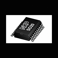
P87LPC769 NXP Semiconductors, P87LPC769 Datasheet - Page 8

P87LPC769
Manufacturer Part Number
P87LPC769
Description
The P87LPC769 is a 20-pin single-chip microcontroller designed forlow pin count applications demanding high-integration, low costsolutions over a wide range of performance requirements
Manufacturer
NXP Semiconductors
Datasheet
1.P87LPC769.pdf
(62 pages)
Available stocks
Company
Part Number
Manufacturer
Quantity
Price
Company:
Part Number:
P87LPC769BD
Manufacturer:
PHILIPS
Quantity:
64
Company:
Part Number:
P87LPC769FD
Manufacturer:
PHILIPS
Quantity:
53
Philips Semiconductors
PIN DESCRIPTIONS
2002 Mar 12
P0.0–P0.7
P1.0–P1.7
MNEMONIC
Low power, low price, low pin count (20 pin)
microcontroller with 4 kB OTP 8-bit A/D, and DAC
2–4, 8–12
1, 13, 14,
PIN NO.
16–20
20
19
18
17
16
14
13
12
10
11
1
9
8
4
3
2
TYPE
I/O
I/O
I/O
I/O
I/O
I/O
O
O
O
O
O
I
I
I
I
I
I
I
I
I
Port 0: Port 0 is an 8-bit I/O port with a user-configurable output type. Port 0 latches are configured in
the quasi-bidirectional mode and have either ones or zeros written to them during reset, as determined
by the PRHI bit in the UCFG1 configuration byte. The operation of port 0 pins as inputs and outputs
depends upon the port configuration selected. Each port pin is configured independently. Refer to the
section on I/O port configuration and the DC Electrical Characteristics for details.
The Keyboard Interrupt feature operates with port 0 pins.
Port 0 also provides various special functions as described below.
Port 1: Port 1 is an 8-bit I/O port with a user-configurable output type, except for three pins as noted
below. Port 1 latches are configured in the quasi-bidirectional mode and have either ones or zeros
written to them during reset, as determined by the PRHI bit in the UCFG1 configuration byte. The
operation of the configurable port 1 pins as inputs and outputs depends upon the port configuration
selected. Each of the configurable port pins are programmed independently. Refer to the section on I/O
port configuration and the DC Electrical Characteristics for details.
Port 1 also provides various special functions as described below.
P0.0
P0.1
P0.2
P0.3
P0.4
P0.5
P0.6
P0.7
P1.0
P1.1
P1.2
P1.3
P1.4
P1.5
P1.6
P1.7
CMP2
CIN2B
CIN2A
CIN1B
AD0
CIN1A
AD1
CMPREF
AD2
CMP1
AD3
T1
TxD
RxD
T0
SCL
INT0
SDA
INT1
RST
DAC1
DAC0
Comparator 2 output.
Comparator 2 positive input B.
Comparator 2 positive input A.
Comparator 1 positive input B.
A/D channel 0 input.
Comparator 1 positive input A.
A/D channel 1 input.
Comparator reference (negative) input.
A/D channel 2 input.
Comparator 1 output.
A/D channel 3 input.
Timer/counter 1 external count input or overflow output.
Transmitter output for the serial port.
Receiver input for the serial port.
Timer/counter 0 external count input or overflow output.
I
drain, in order to conform to I
External interrupt 0 input.
I
drain, in order to conform to I
External interrupt 1 input.
External Reset input (if selected via EPROM configuration). A low on this pin
resets the microcontroller, causing I/O ports and peripherals to take on their
default states, and the processor begins execution at address 0. When used
as a port pin, P1.5 is a Schmitt trigger input only.
Output from Digital to Analog Converter 1
Output from Digital to Analog Converter 0
2
2
C serial clock input/output. When configured as an output, P1.2 is open
C serial data input/output. When configured as an output, P1.3 is open
5
NAME AND FUNCTION
2
2
C specifications.
C specifications.
P87LPC769
Preliminary data


