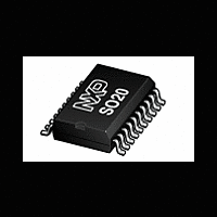
P87LPC769 NXP Semiconductors, P87LPC769 Datasheet - Page 14

P87LPC769
Manufacturer Part Number
P87LPC769
Description
The P87LPC769 is a 20-pin single-chip microcontroller designed forlow pin count applications demanding high-integration, low costsolutions over a wide range of performance requirements
Manufacturer
NXP Semiconductors
Datasheet
1.P87LPC769.pdf
(62 pages)
Available stocks
Company
Part Number
Manufacturer
Quantity
Price
Company:
Part Number:
P87LPC769BD
Manufacturer:
PHILIPS
Quantity:
64
Company:
Part Number:
P87LPC769FD
Manufacturer:
PHILIPS
Quantity:
53
If the Power Down mode is entered while the A/D is running from the
Philips Semiconductors
RC clock frequency of 4.5 MHz (6 MHz - 25%). Minimum times for
RCCLK = 1 use an RC clock frequency of 7.5 MHz (6 MHz + 25%).
Table 1. Example A/D Conversion Times
Note: Do not clock ADC from the RC oscillator when MCU clock is greater than 4 MHz.
The A/D in Power Down and Idle Modes
While using the CPU clock as the A/D clock source, the Idle mode
may be used to conserve power and/or to minimize system noise
during the conversion. CPU operation will resume and Idle mode
terminate automatically when a conversion is complete if the A/D
interrupt is active. In Idle mode, noise from the CPU itself is
eliminated, but noise from the oscillator and any other on-chip
peripherals that are running will remain.
The CPU may be put into Power Down mode when the A/D is
clocked by the on-chip RC oscillator (RCCLK=1). This mode gives
the best possible A/D accuracy by eliminating most on-chip noise
sources.
CPU clock (RCCLK=0), the A/D will abort operation and will not
wake up the CPU. The contents of DAC0 will be invalid when
operation does resume.
2002 Mar 12
Low power, low price, low pin count (20 pin)
microcontroller with 4 kB OTP 8-bit A/D, and DAC
CPU Clock Rate
CPU Clock Rate
32 kHz
1 MHz
4 MHz
AD0 (P0.3)
AD1 (P0.4)
AD2 (P0.5)
AD3 (P0.6)
RCCLK = 0
RCCLK = 0
46.5 s
186 s
AADR1
NA
00
01
10
11
AADR0
Figure 3. A/D Converter Connections
ADCON
minimum
A/D Converter
563.4 s
32.4 s
18.9 s
11
Nominal time assume an ideal RC clock frequency of 6 MHz and an
average of 3.5 machine cycles at the CPU clock rate.
When an A/D conversion is started, Power Down or Idle mode must
be activated within two machine cycles in order to have the most
accurate A/D result. These two machine cycles are counted at the
CPU clock rate. When using the A/D with either Power Down or Idle
mode, care must be taken to insure that the CPU is not restarted by
another interrupt until the A/D conversion is complete. The possible
causes of wakeup are different in Power Down and Idle modes.
A/D accuracy is also affected by noise generated elsewhere in the
application, power supply noise, and power supply regulation. Since
the P87LPC769 power pins are also used as the A/D reference and
supply, the power supply has a very direct affect on the accuracy of
A/D readings. Using the A/D without Power Down mode while the
clock is divided through the use of CLKR or DIVM has an adverse
effect on A/D accuracy.
(A/D result)
DAC0
RCCLK = 1
nominal
39.3 s
23.6 s
659 s
V
V
REF
REF
+ = V
- = V
SS
DD
P87LPC769
maximum
48.9 s
30.1 s
757 s
SU01356
Preliminary data


