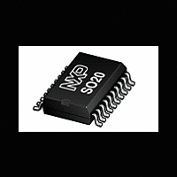
P87LPC769 NXP Semiconductors, P87LPC769 Datasheet - Page 12

P87LPC769
Manufacturer Part Number
P87LPC769
Description
The P87LPC769 is a 20-pin single-chip microcontroller designed forlow pin count applications demanding high-integration, low costsolutions over a wide range of performance requirements
Manufacturer
NXP Semiconductors
Datasheet
1.P87LPC769.pdf
(62 pages)
Available stocks
Company
Part Number
Manufacturer
Quantity
Price
Company:
Part Number:
P87LPC769BD
Manufacturer:
PHILIPS
Quantity:
64
Company:
Part Number:
P87LPC769FD
Manufacturer:
PHILIPS
Quantity:
53
Philips Semiconductors
FUNCTIONAL DESCRIPTION
Details of P87LPC769 functions will be described in the following
sections.
Enhanced CPU
The P87LPC769 uses an enhanced 80C51 CPU which runs at twice
the speed of standard 80C51 devices. This means that the
performance of the P87LPC769 running at 10 MHz is exactly the
same as that of a standard 80C51 running at 20 MHz. A machine
cycle consists of 6 oscillator cycles, and most instructions execute in 6
or 12 clocks. A user configurable option allows restoring standard
80C51 execution timing. In that case, a machine cycle becomes 12
oscillator cycles.
In the following sections, the term “CPU clock” is used to refer to the
clock that controls internal instruction execution. This may
sometimes be different from the externally applied clock, as in the
case where the part is configured for standard 80C51 timing by
means of the CLKR configuration bit or in the case where the clock
is divided down via the setting of the DIVM register. These features
are described in the Oscillator section.
Analog Functions
The P87LPC769 incorporates analog peripheral functions: an
Analog to Digital Converter, two Analog Comparators, and two
Digital to Analog Converters. In order to give the best analog
function performance and to minimize power consumption, pins that
are being used for analog functions must have the digital outputs
and except for the DAC output pins the digital inputs must also be
disabled.
Digital outputs are disabled by putting the port output into the Input
Only (high impedance) mode as described in the I/O Ports section.
Digital inputs on port 0 may be disabled through the use of the
PT0AD register. Each bit in this register corresponds to one pin of
Port 0. Setting the corresponding bit in PT0AD disables that pin’s
digital input. Port bits that have their digital inputs disabled will be
read as 0 by any instruction that accesses the port.
Analog to Digital Converter
The P87LPC769 incorporates a four channel, 8-bit A/D converter.
The A/D inputs are alternate functions on four port 0 pins. Because
2002 Mar 12
Low power, low price, low pin count (20 pin)
microcontroller with 4 kB OTP 8-bit A/D, and DAC
9
the device has a very limited number of pins, the A/D power supply
and references are shared with the processor power pins, V
V
The A/D converter circuitry consists of a 4-input analog multiplexer
and an 8-bit successive approximation ADC. The A/D employs a
ratiometric potentiometer which guarantees DAC monotonicity. The
DAC0 voltage may be output to a pin if the A/D converter is not
enabled. Refer to the section Digital to Analog Converter (DAC)
Outputs for details.
The A/D converter is controlled by the special function register
ADCON. Details of ADCON are shown in Figure 2. The A/D must be
enabled by setting the ENADC bit at least 10 microseconds before a
conversion is started, to allow time for the A/D to stabilize. Prior to
the beginning of an A/D conversion, one analog input pin must be
selected for conversion via the AADR1 and AADR0 bits. These bits
cannot be changed while the A/D is performing a conversion.
An A/D conversion is started by setting the ADCS bit, which remains
set while the conversion is in progress. When the conversion is
complete, the ADCS bit is cleared and the ADCI bit is set. When
ADCI is set, it will generate an interrupt if the interrupt system is
enabled, the A/D interrupt is enabled (via the EAD bit in the IE1
register), and the A/D interrupt is the highest priority pending
interrupt.
When a conversion is complete, the result is contained in the
register DAC0. This value will not change until another conversion is
started. Before another A/D conversion may be started, the ADCI bit
must be cleared by software. The A/D channel selection may be
changed by the same instruction that sets ADCS to start a new
conversion, but not by the same instruction that clears ADCI.
The connections of the A/D converter are shown in Figure 3.
The ideal A/D result may be calculated as follows:
Result
SS
.
(V
IN
–V
SS
) x
V
DD
256
–V
SS
(round result to the nearest integer)
P87LPC769
Preliminary data
DD
and


