LH75401_LH75411_N NXP Semiconductors, LH75401_LH75411_N Datasheet - Page 14

LH75401_LH75411_N
Manufacturer Part Number
LH75401_LH75411_N
Description
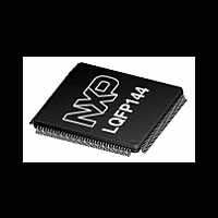
The NXP BlueStreak LH75401/LH75411 family consists of two low-cost 16/32-bit System-on-Chip (SoC) devices
Manufacturer
NXP Semiconductors
Datasheet
1.LH75401_LH75411_N.pdf
(63 pages)
- Current page: 14 of 63
- Download datasheet (666Kb)
LH75401/LH75411
NOTES:
1. These pin numbers have multiplexed functions.
2. Signals preceded with ‘n’ are active LOW.
14
PIN NO. SIGNAL NAME
112
126
134
106
119
127
140
73
74
76
77
78
79
81
82
83
86
87
63
64
65
66
67
68
69
17
34
42
54
98
26
41
48
59
11
75
14
80
70
84
85
88
97
3
8
INT5
INT4
INT3
INT2
INT1
INT0
nPOR
XTAL32IN
XTAL32OUT
XTALIN
XTALOUT
TEST2
TEST1
TMS
RTCK
TCK
TDI
TDO
VDD
VSS
VDDC
VSSC
LINREGEN
VSSA_PLL
VDDA_PLL
VSSA_ADC
VDDA_ADC
Output
Output
Output
Output
Power
Power
Power
Power
Power
Power
Power
Power
TYPE
Input
Input
Input
Input
Input
Input
Input
Input
Input
Input
Input
Input
Input
Input
Input
Table 3. LH75401 Signal Descriptions (Cont’d)
External Interrupt Input 5
External Interrupt Input 4
External Interrupt Input 3
External Interrupt Input 2
External Interrupt Input 1
External Interrupt Input 0
Power-on Reset Input
32.768 kHz Crystal Clock Input
32.768 kHz Crystal Clock Output
Crystal Clock Input
Crystal Clock Output
Test Mode Pin 2
Test Mode Pin 1
JTAG Test Mode Select Input
Returned JTAG Test Clock Output
JTAG Test Clock Input
JTAG Test Serial Data Input
JTAG Test Data Serial Output
I/O Ring VDD
I/O Ring VSS
Core VDD supply (Output if Linear Regulator Enabled, Otherwise Input)
Core VSS
Linear Regulator Enable
PLL Analog VSS
PLL Analog VDD Supply
A-to-D converter Analog VSS
A-to-D converter Analog VDD Supply
POWER AND GROUND (GND)
NXP Semiconductors
Rev. 01 — 16 July 2007
TEST INTERFACE
DESCRIPTION
Preliminary data sheet
System-on-Chip
NOTES
1
1
1
1
1
1
2
Related parts for LH75401_LH75411_N
Image
Part Number
Description
Manufacturer
Datasheet
Request
R
Part Number:
Description:
Lh75401; Lh75411 System-on-chip
Manufacturer:
NXP Semiconductors
Datasheet:
Part Number:
Description:
NXP Semiconductors designed the LPC2420/2460 microcontroller around a 16-bit/32-bitARM7TDMI-S CPU core with real-time debug interfaces that include both JTAG andembedded trace
Manufacturer:
NXP Semiconductors
Datasheet:

Part Number:
Description:
NXP Semiconductors designed the LPC2458 microcontroller around a 16-bit/32-bitARM7TDMI-S CPU core with real-time debug interfaces that include both JTAG andembedded trace
Manufacturer:
NXP Semiconductors
Datasheet:
Part Number:
Description:
NXP Semiconductors designed the LPC2468 microcontroller around a 16-bit/32-bitARM7TDMI-S CPU core with real-time debug interfaces that include both JTAG andembedded trace
Manufacturer:
NXP Semiconductors
Datasheet:
Part Number:
Description:
NXP Semiconductors designed the LPC2470 microcontroller, powered by theARM7TDMI-S core, to be a highly integrated microcontroller for a wide range ofapplications that require advanced communications and high quality graphic displays
Manufacturer:
NXP Semiconductors
Datasheet:
Part Number:
Description:
NXP Semiconductors designed the LPC2478 microcontroller, powered by theARM7TDMI-S core, to be a highly integrated microcontroller for a wide range ofapplications that require advanced communications and high quality graphic displays
Manufacturer:
NXP Semiconductors
Datasheet:
Part Number:
Description:
The Philips Semiconductors XA (eXtended Architecture) family of 16-bit single-chip microcontrollers is powerful enough to easily handle the requirements of high performance embedded applications, yet inexpensive enough to compete in the market for hi
Manufacturer:
NXP Semiconductors
Datasheet:
Part Number:
Description:
The XA-S3 device is a member of Philips Semiconductors? XA(eXtended Architecture) family of high performance 16-bitsingle-chip microcontrollers
Manufacturer:
NXP Semiconductors
Datasheet:

Part Number:
Description:
The NXP LPC3130/3131 combine an 180 MHz ARM926EJ-S CPU core, high-speed USB2
Manufacturer:
NXP Semiconductors
Datasheet:

Part Number:
Description:
The NXP LPC3141 combine a 270 MHz ARM926EJ-S CPU core, High-speed USB 2
Manufacturer:
NXP Semiconductors

Part Number:
Description:
The NXP LPC3143 combine a 270 MHz ARM926EJ-S CPU core, High-speed USB 2
Manufacturer:
NXP Semiconductors

Part Number:
Description:
The NXP LPC3152 combines an 180 MHz ARM926EJ-S CPU core, High-speed USB 2
Manufacturer:
NXP Semiconductors

Part Number:
Description:
The NXP LPC3154 combines an 180 MHz ARM926EJ-S CPU core, High-speed USB 2
Manufacturer:
NXP Semiconductors

Part Number:
Description:
Standard level N-channel enhancement mode Field-Effect Transistor (FET) in a plastic package using NXP High-Performance Automotive (HPA) TrenchMOS technology
Manufacturer:
NXP Semiconductors
Datasheet:


