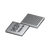
LPC1820FET100 NXP Semiconductors, LPC1820FET100 Datasheet - Page 152

LPC1820FET100
Manufacturer Part Number
LPC1820FET100
Description
The LPC1820FET100 is a high-performance, cost-effective Cortex-M3 microcontroller featuring 168 kB of SRAM, and advanced peripherals including High Speed USB 2
Manufacturer
NXP Semiconductors
Datasheet
1.LPC1810FBD144.pdf
(157 pages)
Available stocks
Company
Part Number
Manufacturer
Quantity
Price
Company:
Part Number:
LPC1820FET100
Manufacturer:
Signetics
Quantity:
45
- Current page: 152 of 157
- Download datasheet (3Mb)
NXP Semiconductors
Table 35.
LPC1850_30_20_10
Preliminary data sheet
Document ID
LPC1850_30_20_10 v.2
Modifications:
Revision history
…continued
Release date Data sheet status
20110713
•
•
•
•
•
•
•
•
•
•
•
•
•
•
•
•
Power consumption data added (Figure 12 to Figure 17).
Pin PC_0 in Table 3: function ENET_RX_CLK changed to n.c. and function
SDIO_CLK changed to function ENET_RX_CLK.
Pin PC_8 in Table 3: ENET_RX_DV applies to RMII/MII interfaces.
Rename pins CAN1_RD and CAN1_TD to CAN0_RD and CAN0_TD in Table 3.
Rename all I2S pins to I2S0 pins.
Condition for RTC operation updated in Table 8, Table note 2.
Figure 11 “LPC1850/30/20/10 Power domains” added.
“n.c.” changed to “Reserved” in Table 3.
Section 11.6: characterization parameters and timing diagrams updated.
Prefix for all SD/MMC pins changed to “SD” in Table 3.
Prefix for all EMC pins changed to “EMC” in Table 3.
Section 11.4 added.
Section 11.8 added.
Section 11.9 added.
LQFP144 pinout added in Table 3.
Updates related to the Rev ‘A’ version of parts LPC1850/30/20/10:
– Pin P6_0 in Table 3: function I2S_RX_SCK moved to function level 5.
– Pin PF_0 in Table 3: function GP_CLKIN added.
– Pin PA_1 in Table 3: function U2_TXD added.
– Pin PA_2 in Table 3: function U2_RXD added.
– Pin PC_0 in Table 3: reset state changed to I; PU.
– Pin P1_16 in Table 3: ENET_CRS_DV moved to function level 7.
– Pad descriptions updated in Table 3, Table note 3 to Table note 11.
– Added function levels four to seven/eight for each pin in Table 3.
– Second C_CAN interface (C_CAN1) added.
– Second I
– Audio PLL added (Section 2 and Section 7.18.6).
– All SDIO functions moved to the function levels four to seven in Table 3.
– High-speed GPIO block moved to address 0x400F 4000 in Figure 9 and
– GPIO interrupts and GPIO group0 and group1 interrupt added in Figure 1,
– Number of GPIO ports increased to eight.
– Total number of GPIO pins increased to 164.
– GIMA block added (Section 7.6).
– Band gap output added to pin PF_7.
– Package outline and soldering information added for all packages.
Figure 10.
Figure 9, Figure 10, Section 2, and Section 7.12.
All information provided in this document is subject to legal disclaimers.
Rev. 3.1 — 15 December 2011
Objective data sheet
2
S interface (I2S1) added.
Change notice Supersedes
-
32-bit ARM Cortex-M3 microcontroller
LPC1850/30/20/10
LPC1850_30_20_10 v.1.2
© NXP B.V. 2011. All rights reserved.
152 of 157
Related parts for LPC1820FET100
Image
Part Number
Description
Manufacturer
Datasheet
Request
R
Part Number:
Description:
NXP Semiconductors designed the LPC2420/2460 microcontroller around a 16-bit/32-bitARM7TDMI-S CPU core with real-time debug interfaces that include both JTAG andembedded trace
Manufacturer:
NXP Semiconductors
Datasheet:

Part Number:
Description:
NXP Semiconductors designed the LPC2458 microcontroller around a 16-bit/32-bitARM7TDMI-S CPU core with real-time debug interfaces that include both JTAG andembedded trace
Manufacturer:
NXP Semiconductors
Datasheet:
Part Number:
Description:
NXP Semiconductors designed the LPC2468 microcontroller around a 16-bit/32-bitARM7TDMI-S CPU core with real-time debug interfaces that include both JTAG andembedded trace
Manufacturer:
NXP Semiconductors
Datasheet:
Part Number:
Description:
NXP Semiconductors designed the LPC2470 microcontroller, powered by theARM7TDMI-S core, to be a highly integrated microcontroller for a wide range ofapplications that require advanced communications and high quality graphic displays
Manufacturer:
NXP Semiconductors
Datasheet:
Part Number:
Description:
NXP Semiconductors designed the LPC2478 microcontroller, powered by theARM7TDMI-S core, to be a highly integrated microcontroller for a wide range ofapplications that require advanced communications and high quality graphic displays
Manufacturer:
NXP Semiconductors
Datasheet:
Part Number:
Description:
The Philips Semiconductors XA (eXtended Architecture) family of 16-bit single-chip microcontrollers is powerful enough to easily handle the requirements of high performance embedded applications, yet inexpensive enough to compete in the market for hi
Manufacturer:
NXP Semiconductors
Datasheet:
Part Number:
Description:
The XA-S3 device is a member of Philips Semiconductors? XA(eXtended Architecture) family of high performance 16-bitsingle-chip microcontrollers
Manufacturer:
NXP Semiconductors
Datasheet:

Part Number:
Description:
The NXP BlueStreak LH75401/LH75411 family consists of two low-cost 16/32-bit System-on-Chip (SoC) devices
Manufacturer:
NXP Semiconductors
Datasheet:

Part Number:
Description:
The NXP LPC3130/3131 combine an 180 MHz ARM926EJ-S CPU core, high-speed USB2
Manufacturer:
NXP Semiconductors
Datasheet:

Part Number:
Description:
The NXP LPC3141 combine a 270 MHz ARM926EJ-S CPU core, High-speed USB 2
Manufacturer:
NXP Semiconductors

Part Number:
Description:
The NXP LPC3143 combine a 270 MHz ARM926EJ-S CPU core, High-speed USB 2
Manufacturer:
NXP Semiconductors

Part Number:
Description:
The NXP LPC3152 combines an 180 MHz ARM926EJ-S CPU core, High-speed USB 2
Manufacturer:
NXP Semiconductors

Part Number:
Description:
The NXP LPC3154 combines an 180 MHz ARM926EJ-S CPU core, High-speed USB 2
Manufacturer:
NXP Semiconductors

Part Number:
Description:
Standard level N-channel enhancement mode Field-Effect Transistor (FET) in a plastic package using NXP High-Performance Automotive (HPA) TrenchMOS technology
Manufacturer:
NXP Semiconductors
Datasheet:


