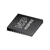
LPC1343FHN33 NXP Semiconductors, LPC1343FHN33 Datasheet - Page 29

LPC1343FHN33
Manufacturer Part Number
LPC1343FHN33
Description
The LPC1343FHN33 is a ARM Cortex-M3 based microcontroller for embedded applications featuring a high level of integration and low power consumption
Manufacturer
NXP Semiconductors
Datasheet
1.LPC1311FHN33.pdf
(73 pages)
Available stocks
Company
Part Number
Manufacturer
Quantity
Price
Company:
Part Number:
LPC1343FHN33
Manufacturer:
SG
Quantity:
200
Part Number:
LPC1343FHN33
Manufacturer:
NXP/恩智浦
Quantity:
20 000
Company:
Part Number:
LPC1343FHN33,551
Manufacturer:
NXP
Quantity:
780
NXP Semiconductors
LPC1311_13_42_43
Product data sheet
CAUTION
7.19.5 Boot loader
7.19.6 APB interface
7.19.7 AHB-Lite
7.19.8 External interrupt inputs
7.19.9 Memory mapping control
There are three levels of Code Read Protection:
The boot loader controls initial operation after reset and also provides the means to
program the flash memory. This could be initial programming of a blank device, erasure
and re-programming of a previously programmed device, or programming of the flash
memory by the application program in a running system.
The boot loader code is executed every time the part is reset or powered up. The loader
can either execute the ISP command handler or the user application code, or, on the
LPC1342/43, it can program the flash image via an attached MSC device through USB
(Windows operating system only). A LOW level during reset applied to the PIO0_1 pin is
considered as an external hardware request to start the ISP command handler or the USB
device enumeration. The state of PIO0_3 determines whether the UART or USB interface
will be used (LPC1342/43 only).
The APB peripherals are located on one APB bus.
The AHB-Lite connects the instruction (I-code) and data (D-code) CPU buses of the ARM
Cortex-M3 to the flash memory, the main static RAM, and the boot ROM.
All GPIO pins can be level or edge sensitive interrupt inputs. In addition, start logic inputs
serve as external interrupts (see
The Cortex-M3 incorporates a mechanism that allows remapping the interrupt vector table
to alternate locations in the memory map. This is controlled via the Vector Table Offset
Register contained in the NVIC.
1. CRP1 disables access to chip via the SWD and allows partial flash update (excluding
2. CRP2 disables access to chip via the SWD and only allows full flash erase and
3. Running an application with level CRP3 selected fully disables any access to chip via
flash sector 0) using a limited set of the ISP commands. This mode is useful when
CRP is required and flash field updates are needed but all sectors can not be erased.
update using a reduced set of the ISP commands.
the SWD pins and the ISP. This mode effectively disables ISP override using PIO0_1
pin, too. It is up to the user’s application to provide (if needed) flash update
mechanism using IAP calls or call reinvoke ISP command to enable flash update via
UART.
If level three Code Read Protection (CRP3) is selected, no future factory testing can be
performed on the device.
All information provided in this document is subject to legal disclaimers.
Rev. 4 — 20 June 2011
Section
7.19.1).
32-bit ARM Cortex-M3 microcontroller
LPC1311/13/42/43
© NXP B.V. 2011. All rights reserved.
29 of 73


