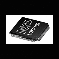
LPC12D27FBD100 NXP Semiconductors, LPC12D27FBD100 Datasheet - Page 2

LPC12D27FBD100
Manufacturer Part Number
LPC12D27FBD100
Description
The LPC12D27FBD100 is a ARM Cortex-M0 based microcontroller for embedded applications featuring a high level of integration and low power consumption
Manufacturer
NXP Semiconductors
Datasheet
1.LPC12D27FBD100.pdf
(46 pages)
Available stocks
Company
Part Number
Manufacturer
Quantity
Price
Company:
Part Number:
LPC12D27FBD100/301
Manufacturer:
NXP Semiconductors
Quantity:
10 000
NXP Semiconductors
LPC12D27
Product data sheet
Clock generation unit
Digital peripherals
Analog peripherals
Power
Unique device serial number for identification.
3.3 V power supply.
Available as 100-pin LQFP package.
In-System Programming (ISP) and In-Application Programming (IAP) via on-chip
bootloader software.
Includes ROM-based 32-bit integer division routines.
Crystal oscillator with an operating range of 1 MHz to 25 MHz.
12 MHz Internal RC (IRC) oscillator trimmed to 1 % accuracy that can optionally be
used as a system clock.
PLL allows CPU operation up to the maximum CPU rate without the need for a
high-frequency crystal. May be run from the system oscillator or the internal RC
oscillator.
Clock output function with divider that can reflect the system oscillator clock, IRC
clock, main clock, and Watchdog clock.
Real-Time Clock (RTC).
Micro DMA controller with 21 channels.
CRC engine.
Two UARTs with fractional baud rate generation and internal FIFO. One UART with
RS-485 and modem support and one standard UART with IrDA.
SSP/SPI controller with FIFO and multi-protocol capabilities.
I
data rate of 1 Mbit/s with multiple address recognition and monitor mode. I
pins have programmable glitch filter.
Up to 40 General Purpose I/O (GPIO) pins with programmable pull-up resistor,
open-drain mode, programmable digital input glitch filter, and programmable input
inverter.
Programmable output drive on all GPIO pins. Four pins support high-current output
drivers.
All GPIO pins can be used as edge and level sensitive interrupt sources.
Four general purpose counter/timers with four capture inputs and four match
outputs (32-bit timers) or two capture inputs and two match outputs (16-bit timers).
Windowed WatchDog Timer (WWDT), IEC-60335 Class B certified.
One 8-channel, 10-bit ADC.
Two highly flexible analog comparators. Comparator outputs can be programmed
to trigger a timer match signal or can be used to emulate 555 timer behavior.
Three reduced power modes: Sleep, Deep-sleep, and Deep power-down.
Processor wake-up from Deep-sleep mode via start logic using 12 port pins.
Processor wake-up from Deep-power down and Deep-sleep modes via the RTC.
Brownout detect with three separate thresholds each for interrupt and forced reset.
Power-On Reset (POR).
Integrated PMU (Power Management Unit).
2
C-bus interface supporting full I
All information provided in this document is subject to legal disclaimers.
Rev. 1 — 20 September 2011
2
C-bus specification and Fast-mode Plus with a
32-bit ARM Cortex-M0 microcontroller
LPC12D27
© NXP B.V. 2011. All rights reserved.
2
C-bus
2 of 46


