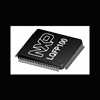
LPC12D27FBD100 NXP Semiconductors, LPC12D27FBD100 Datasheet - Page 11

LPC12D27FBD100
Manufacturer Part Number
LPC12D27FBD100
Description
The LPC12D27FBD100 is a ARM Cortex-M0 based microcontroller for embedded applications featuring a high level of integration and low power consumption
Manufacturer
NXP Semiconductors
Datasheet
1.LPC12D27FBD100.pdf
(46 pages)
Available stocks
Company
Part Number
Manufacturer
Quantity
Price
Company:
Part Number:
LPC12D27FBD100/301
Manufacturer:
NXP Semiconductors
Quantity:
10 000
NXP Semiconductors
Table 3.
LPC12D27
Product data sheet
Symbol
SWDIO/ACMP1_I2/
CT32B1_CAP2/
CT32B1_MAT2/PIO0_25
SWCLK/
ACMP1_I3/
CT32B1_CAP3/
CT32B1_MAT3/PIO0_26
PIO0_27/ACMP0_O
PIO0_28/ACMP1_O/
CT16B0_CAP0/
CT16B0_MAT0
PIO0_29/ROSC/
CT16B0_CAP1/
CT16B0_MAT1
R/PIO0_30/AD0
R/PIO0_31/AD1
PIO1_0 to PIO1_6
R/PIO1_0/AD2
LPC12D27 LQFP100 pin description
Pin
1
2
3
4
5
26
27
28
[5]
[5]
[7]
[7]
[7]
[5]
[5]
[5]
Start
logic
input
no
no
no
no
no
no
no
no
Reset
state
[1]
I; PU
I; PU
I; PU
I; PU
I; PU
I; PU
I; PU
I; PU
All information provided in this document is subject to legal disclaimers.
Rev. 1 — 20 September 2011
Type
I/O
I
I
O
I/O
I
I
I
O
I/O
I/O
O
I/O
O
I
O
I/O
I/O
I
O
I
I/O
I
I
I/O
I
I/O
O
I/O
I
…continued
Description
SWDIO — Serial wire debug input/output, default location.
ACMP1_I2 — Input 2 for comparator 1.
CT32B1_CAP2 — Capture input, channel 2 for 32-bit timer 1.
CT32B1_MAT2 — Match output, channel 2 for 32-bit timer 1.
PIO0_25 — General purpose digital input/output pin.
SWCLK — Serial wire clock, default location.
ACMP1_I3 — Input 3 for comparator 1.
CT32B1_CAP3 — Capture input, channel 3 or 32-bit timer 1.
CT32B1_MAT3 — Match output, channel 3 for 32-bit timer 1.
PIO0_26 — General purpose digital input/output pin.
PIO0_27 — General purpose digital input/output pin
(high-current output driver).
ACMP0_O — Output for comparator 0.
PIO0_28 — General purpose digital input/output pin
(high-current output driver).
ACMPC1_O — Output for comparator 1.
CT16B0_CAP0 — Capture input, channel 0 for 16-bit timer 0.
CT16B0_MAT0 — Match output, channel 0 for 16-bit timer 0.
PIO0_29 — General purpose digital input/output pin
(high-current output driver).
ROSC — Relaxation oscillator for 555 timer applications.
CT16B0_CAP1 — Capture input, channel 1 for 16-bit timer 0.
CT16B0_MAT1 — Match output, channel 1 for 16-bit timer 0.
R — Reserved. Configure for an alternate function in the
IOCONFIG block.
PIO0_30 — General purpose digital input/output pin.
AD0 — A/D converter, input 0.
R — Reserved. Configure for an alternate function in the
IOCONFIG block.
PIO0_31 — General purpose digital input/output pin.
AD1 — A/D converter, input 1.
Port 1 — Port 1 is a 32-bit I/O port with individual direction and
function controls for each bit. The operation of port 1 pins
depends on the function selected through the IOCONFIG register
block. Pins PIO1_7 through PIO1_31 are not available.
R — Reserved. Configure for an alternate function in the
IOCONFIG block.
PIO1_0 — General purpose digital input/output pin.
AD2 — A/D converter, input 2.
32-bit ARM Cortex-M0 microcontroller
LPC12D27
© NXP B.V. 2011. All rights reserved.
11 of 46


