MAX9742ETX+ Maxim Integrated Products, MAX9742ETX+ Datasheet - Page 5
MAX9742ETX+
Manufacturer Part Number
MAX9742ETX+
Description
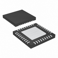
IC AMP AUDIO PWR 20.5W D 36TQFN
Manufacturer
Maxim Integrated Products
Type
Class Dr
Datasheet
1.MAX9742ETX.pdf
(36 pages)
Specifications of MAX9742ETX+
Output Type
2-Channel (Stereo)
Max Output Power X Channels @ Load
20.5W x 2 @ 8 Ohm
Voltage - Supply
20 V ~ 40 V, ±10 V ~ 20 V
Features
Depop, Differential Inputs, Mute, Short-Circuit and Thermal Protection, Shutdown
Mounting Type
Surface Mount
Package / Case
36-TQFN Exposed Pad
Product
Class-D
Output Power
16 W
Thd Plus Noise
0.08 %
Supply Current
15 mA
Maximum Power Dissipation
2.86 W
Maximum Operating Temperature
+ 85 C
Mounting Style
SMD/SMT
Audio Load Resistance
4 Ohms
Minimum Operating Temperature
- 40 C
Lead Free Status / RoHS Status
Lead free / RoHS Compliant


ELECTRICAL CHARACTERISTICS—Single-Supply, BTL Configuration
(V
10kΩ, C
= 121kΩ, R
+25°C.) (Note 2)
Note 2: All devices are 100% production tested at +25°C. All temperature limits are guaranteed by design.
Note 3: Supply pumping may occur at high output powers with low audio frequencies. Use proper supply bypassing to prevent the
Note 4: Amplifier inputs AC-coupled to ground.
Note 5: For R
Note 6: Testing performed with four-layer PCB.
Note 7: Both channels driven in phase.
Note 8: Testing performed with an 8Ω resistor connected between LC filter output and ground. Mode transitions are controlled by
Note 9: Digital input specifications apply to both single-supply and dual-supply operation.
Note 10: Channels driven 180° out-of-phase. Load connected between LC filter outputs.
Note 11: L
Note 12: Testing performed with an 8Ω resistor connected between LC filter outputs. Mode transitions are controlled by SHDN. K
Output Offset Voltage
Power-Supply Rejection Ratio
(Note 4)
Continuous Output Power
Efficiency
Total Harmonic Distortion Plus
Noise (Notes 6, 10, and 11)
Signal-to-Noise Ratio
Shutdown-to-Full Operation
Click-and-Pop
DD
= 24V, V
SFT
PARAMETER
device from entering overvoltage protection due to supply pumping. See the Supply Pumping Effects and the Supply
Undervoltage and Overvoltage Protection sections.
0.33µF.
SHDN. K
level is calculated as 20log[(peak voltage during mode transition, no input signal) / 1V
F
F1B
= 0.47µF, C
= 22µH and C
SS
L
= 562kΩ, R
= 4Ω, L
= V
CP
Class D Amplifier with Differential Inputs
_______________________________________________________________________________________
SUB
level is calculated as 20log[(peak voltage during mode transition, no input signal) / 1V
OUT
F
= LGND = 0V, V
= 22µH and C
F
F2
= 0.68µF.
= 1000µF, C
= 681kΩ, R
SYMBOL
THD+N
PSRR
P
SNR
t
K
SON
OUT
CP
F
FB_1
REF
= 0.68µF. For R
SHDN
Single-/Dual-Supply, Stereo 16W,
= 68kΩ, R
(Note 4)
V
V
R
(Notes 6, 10, and 11)
R
(Notes 5 and 6)
f
R
P
BW = 22Hz to 22kHz
(Notes 6, 10, and 11)
P eak vol tag e, 32- sam p l es
p er second , A- w ei g hted
( N otes 4, 11, and 12)
= 150pF, C
IN
DD
DD
L
L
L
OUT
= 3.3V, V
= 8Ω, f
= 8Ω, P
= 1kHz, BW = 22Hz to 22kHz,
= 8Ω, P
= 20V to 40V
= 24V + 500mV
= 32W, R
IN
L
OUT
OUT
L
FB_2
= ∞, T
MID
= 1kHz, THD+N = 10%,
= 6Ω, L
L
= 10W, THD+N = 10%,
= 10W
= 12V, C
= 10pF, C
= 8Ω,
A
CONDITIONS
= T
P-P
F
= 33µH and C
, f = 1kHz
MIN
VDD
BOOT
to T
Unweighted
A-weighted
Into shutdown
Out of shutdown
= 660µF, C
MAX
= 0.1µF, C
, unless otherwise noted. Typical values are at T
F
= 0.47µF. For R
MID1
REGP
= 10µF, C
= C
RMS
REGM
].
L
MIN
= 8Ω, L
MID2
= 1µF, R
RMS
= 10µF, R1 = R2 = R3 =
TYP
0.08
F
-47
-32
88
77
32
83
90
96
68
7
= 47µH and C
].
IN_
MAX
= 30.1kΩ, R
F
UNITS
=
dBV
mV
dB
dB
ms
W
%
%
CP
F1A
A
5
=
Related parts for MAX9742ETX+
Image
Part Number
Description
Manufacturer
Datasheet
Request
R

Part Number:
Description:
Max9742 Single-/dual-supply, Stereo 16w, Class D Amplifier With Differential Inputs
Manufacturer:
Maxim Integrated Products, Inc.
Datasheet:

Part Number:
Description:
MAX7528KCWPMaxim Integrated Products [CMOS Dual 8-Bit Buffered Multiplying DACs]
Manufacturer:
Maxim Integrated Products
Datasheet:
Part Number:
Description:
Single +5V, fully integrated, 1.25Gbps laser diode driver.
Manufacturer:
Maxim Integrated Products
Datasheet:
Part Number:
Description:
Single +5V, fully integrated, 155Mbps laser diode driver.
Manufacturer:
Maxim Integrated Products
Datasheet:
Part Number:
Description:
VRD11/VRD10, K8 Rev F 2/3/4-Phase PWM Controllers with Integrated Dual MOSFET Drivers
Manufacturer:
Maxim Integrated Products
Datasheet:
Part Number:
Description:
Highly Integrated Level 2 SMBus Battery Chargers
Manufacturer:
Maxim Integrated Products
Datasheet:
Part Number:
Description:
Current Monitor and Accumulator with Integrated Sense Resistor; ; Temperature Range: -40°C to +85°C
Manufacturer:
Maxim Integrated Products
Part Number:
Description:
TSSOP 14/A�/RS-485 Transceivers with Integrated 100O/120O Termination Resis
Manufacturer:
Maxim Integrated Products
Part Number:
Description:
TSSOP 14/A�/RS-485 Transceivers with Integrated 100O/120O Termination Resis
Manufacturer:
Maxim Integrated Products
Part Number:
Description:
QFN 16/A�/AC-DC and DC-DC Peak-Current-Mode Converters with Integrated Step
Manufacturer:
Maxim Integrated Products
Part Number:
Description:
TDFN/A/65V, 1A, 600KHZ, SYNCHRONOUS STEP-DOWN REGULATOR WITH INTEGRATED SWI
Manufacturer:
Maxim Integrated Products
Part Number:
Description:
Integrated Temperature Controller f
Manufacturer:
Maxim Integrated Products
Part Number:
Description:
SOT23-6/I�/45MHz to 650MHz, Integrated IF VCOs with Differential Output
Manufacturer:
Maxim Integrated Products
Part Number:
Description:
SOT23-6/I�/45MHz to 650MHz, Integrated IF VCOs with Differential Output
Manufacturer:
Maxim Integrated Products
Part Number:
Description:
EVALUATION KIT/2.4GHZ TO 2.5GHZ 802.11G/B RF TRANSCEIVER WITH INTEGRATED PA
Manufacturer:
Maxim Integrated Products