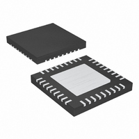
MAX9742ETX+ Maxim Integrated Products, MAX9742ETX+ Datasheet - Page 29

MAX9742ETX+
Manufacturer Part Number
MAX9742ETX+
Description
IC AMP AUDIO PWR 20.5W D 36TQFN
Manufacturer
Maxim Integrated Products
Type
Class Dr
Datasheet
1.MAX9742ETX.pdf
(36 pages)
Specifications of MAX9742ETX+
Output Type
2-Channel (Stereo)
Max Output Power X Channels @ Load
20.5W x 2 @ 8 Ohm
Voltage - Supply
20 V ~ 40 V, ±10 V ~ 20 V
Features
Depop, Differential Inputs, Mute, Short-Circuit and Thermal Protection, Shutdown
Mounting Type
Surface Mount
Package / Case
36-TQFN Exposed Pad
Product
Class-D
Output Power
16 W
Thd Plus Noise
0.08 %
Supply Current
15 mA
Maximum Power Dissipation
2.86 W
Maximum Operating Temperature
+ 85 C
Mounting Style
SMD/SMT
Audio Load Resistance
4 Ohms
Minimum Operating Temperature
- 40 C
Lead Free Status / RoHS Status
Lead free / RoHS Compliant
To maximize output power and minimize distortion,
proper layout and supply bypassing is essential. To
prevent ground-loop-induced noise and minimize noise
due to parasitic ground inductance, use separate
ground planes for input-signal ground connections
(SGND plane) and output-power ground connections
(PGND plane). For dual-supply applications, connect
MID to the SGND plane. For single-supply operation,
connect MID to an external voltage-divider and bypass
MID to the SGND plane with a decoupling network (see
Figure 11). This provides a sufficient low- and high-fre-
quency AC ground for the internal amplifiers. Connect
the SGND and PGND planes together at a single point
in the PCB near the MAX9742. Minimize the parasitic
trace inductances and resistances associated with the
V
imal length.
Proper power-supply bypassing is essential to ensure
low distortion operation and to prevent excessive sup-
ply pumping when using the single-ended output con-
figuration. For dual-supply operation, bypass V
V
itors. V
with 0.1µF capacitors as physically close as possible to
V
decoupling. Also, connect an additional 1µF capacitor
between V
bypass V
should also be bypassed to PGND with an additional
0.1µF capacitor as physically close as possible to the
V
The MAX9742 includes voltage regulators for the inter-
nal amplifiers, logic circuitry, and gate-drive circuitry
that require external bypassing. Bypass REGP and
REGM to the SGND plane with 1µF capacitors. Bypass
REGLS to NSENSE with a 1µF capacitor. Bypass LV
to LGND with a 0.1µF capacitor. The voltage rating
requirements of the external bypass capacitors must
be taken into account. This is especially important
when selecting the REGP and REGM bypass capaci-
tors since the ground-referenced voltages present at
these regulator outputs are dependent on the voltage
applied to the MID input. The minimum required volt-
age ratings for the regulator bypass capacitors are
summarized in Table 4.
DD
SS
DD
DD
to PGND with 1000µF aluminum electrolytic capac-
and V
pin.
and V
DD
DD
SS
and V
SS
DD
to PGND with two 330µF capacitors. V
connections, by using wide traces of min-
pins to provide sufficient high-frequency
and V
SS
Class D Amplifier with Differential Inputs
______________________________________________________________________________________
should also be bypassed to PGND
SS
Supply Bypassing/Layout
. For single-supply operation,
Single-/Dual-Supply, Stereo 16W,
DD
and
DD
DD
Class D amplifiers provide much better efficiency and
thermal performance than a comparable Class AB
amplifier. However, the system’s thermal performance
must be considered with realistic expectations along
with its many parameters.
When a Class D amplifier is evaluated in the lab, often
a continuous sine wave is used as the signal source.
While this is convenient for measurement purposes, it
represents a worst-case scenario for thermal loading
on the amplifier. It is not uncommon for a Class D
amplifier to enter thermal shutdown if driven near maxi-
mum output power with a continuous sine wave. The
PCB must be optimized for best dissipation (see the
PCB Thermal Considerations section). Audio content,
both music and voice, has a much lower RMS value rel-
ative to its peak output power. Therefore, while an
audio signal may reach similar peaks as a continuous
sine wave, the actual thermal impact on the Class D
amplifier is highly reduced. If the thermal performance
of a system is being evaluated, it is important to use
actual audio signals instead of sine waves for testing. If
sine waves must be used, the thermal performance is
less than the system’s actual capability for real music
or voice.
The exposed paddle is the primary route for conducting
heat away from the IC. With a bottom-side exposed pad-
dle, the PCB and its copper becomes the primary
heatsink for the Class D amplifier. Solder the exposed
paddle to a copper polygon. Add as much copper as
possible from this polygon to any adjacent pin on the
Class D amplifier as well as to any adjacent components,
provided these connections are at the same potential.
Table 4. Minimum Required Voltage
Ratings for Regulator Bypass Capacitors
CAPACITOR
C
C
C
C
REGLS
REGM
REGP
LVDD
Continuous Sine Wave vs. Music
Thermal Considerations
PCB Thermal Considerations
VOLTAGE RATING (V)
V
V
MID
MID
7
5
+ 5
- 5
29


