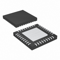
MAX9742ETX+ Maxim Integrated Products, MAX9742ETX+ Datasheet - Page 23

MAX9742ETX+
Manufacturer Part Number
MAX9742ETX+
Description
IC AMP AUDIO PWR 20.5W D 36TQFN
Manufacturer
Maxim Integrated Products
Type
Class Dr
Datasheet
1.MAX9742ETX.pdf
(36 pages)
Specifications of MAX9742ETX+
Output Type
2-Channel (Stereo)
Max Output Power X Channels @ Load
20.5W x 2 @ 8 Ohm
Voltage - Supply
20 V ~ 40 V, ±10 V ~ 20 V
Features
Depop, Differential Inputs, Mute, Short-Circuit and Thermal Protection, Shutdown
Mounting Type
Surface Mount
Package / Case
36-TQFN Exposed Pad
Product
Class-D
Output Power
16 W
Thd Plus Noise
0.08 %
Supply Current
15 mA
Maximum Power Dissipation
2.86 W
Maximum Operating Temperature
+ 85 C
Mounting Style
SMD/SMT
Audio Load Resistance
4 Ohms
Minimum Operating Temperature
- 40 C
Lead Free Status / RoHS Status
Lead free / RoHS Compliant
To provide sufficient gate drive voltage to the high-side
transistor of the half-bridge output stage, an external
diode (D
the internal bootstrapping circuitry (see Figure 2). To
maintain high power efficiencies and maximum output
power at low audio frequencies, use fast-recovery
switching diodes for D
to 1N914, BAS16, or 1N4148 work well.
For most applications, use a C
and ≤ 0.22µF. For proper operation, use capacitors with
low ESR and voltage ratings greater than 7V for C
The MAX9742 requires output-coupling capacitors for
single-supply operation. Since the MAX9742 outputs
switch between V
tion, there is a DC component equal to 0.5 x V
sent at the outputs. The output-coupling capacitor
blocks this DC component, preventing DC current from
flowing into the load. The output capacitor and the load
resistance of the speaker form a highpass filter. The
-3dB point of the highpass filter can be approximated by:
where f
R
the value of the output-coupling capacitor. As with the
input capacitor, choose C
below the lowest frequency of interest. Setting f
high affects the amplifier‘s low-frequency response.
Select capacitors with low ESR to minimize power loss-
es. Since the output-coupling capacitor has a large
amplitude AC current (resulting average output current
due to the LC filter) flowing through it at high output
powers, it is important to select an output-coupling
SPKR
(C
is the DC resistance of the speaker, and C
-3dB
OUT
BOOT
f
−
3dB
, Single-Ended, Single-Supply Operation)
is the -3dB cutoff frequency of the filter,
) and capacitor (C
=
Class D Amplifier with Differential Inputs
DD
______________________________________________________________________________________
2
π
and ground in single-supply opera-
×
BOOT
R
Output-Coupling Capacitors
SPKR
OUT
. Silicon diodes equivalent
Bootstrap Diode (D
1
BOOT
×
such that f
BOOT
C
Capacitor (C
OUT
capacitor ≥ 0.1µF
Single-/Dual-Supply, Stereo 16W,
) are needed for
(
Hz
-3dB
)
-3dB
DD
BOOT
BOOT
is well
OUT
BOOT
pre-
too
is
)
)
.
capacitor that has an appropriate ripple current rating.
To prevent damage to the output-coupling capacitor,
use the following equation to calculate the required
RMS ripple current rating for C
where I
current rating for C
of the speaker. The ripple current ratings of capacitors
are frequency dependent, so be sure to select a
capacitor based on its ripple current rating within the
audio frequency range.
Select output-coupling capacitors with DC voltage rat-
ings greater than V
In single-supply operation with single-ended outputs, the
leakage current of C
the MAX9742. To minimize startup time delays due to
C
than 1µA for C
section for more information on optimizing the startup
time of the MAX9742.
The voltage present at the MID input biases the internal
amplifiers and should be set to the average value of
V
supply operation, connect MID to ground. For single-
supply operation, set MID to 0.5 x V
external resistive divider. To minimize power dissipation
while providing enough input bias current for the MID
input, select divider-resistors with values greater than
or equal to 10kΩ and less than or equal to 20kΩ.
Connect a decoupling network between MID and the
SGND plane (see the Supply Bypassing/Layout sec-
tion) to provide a sufficient low- and high-frequency AC
ground for the internal amplifiers. Figure 11 shows the
recommended decoupling networks for bypassing the
MID input.
DD
OUT
and V
, use capacitors with leakage current ratings less
RMS_RIPPLE
I
RMS_RIPPLE
SS
OUT
for maximum dynamic range. For dual-
. See the Startup Time Considerations
OUT
DD
is the minimum required RMS ripple
OUT
.
=
and R
can affect the startup time of
2.83
SPKR
OUT
V
×
DD
R
:
is the DC resistance
SPKR
DD
( ) A
Setting V
through an
MID
23


