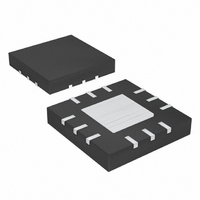
MAX9725AETC+T Maxim Integrated Products, MAX9725AETC+T Datasheet - Page 11

MAX9725AETC+T
Manufacturer Part Number
MAX9725AETC+T
Description
IC AMP AUDIO .025W STER 12TQFN
Manufacturer
Maxim Integrated Products
Series
DirectDrive™r
Type
Class ABr
Datasheet
1.MAX9725CETCT.pdf
(17 pages)
Specifications of MAX9725AETC+T
Output Type
Headphones, 2-Channel (Stereo)
Max Output Power X Channels @ Load
25mW x 2 @ 16 Ohm
Voltage - Supply
900 mV ~ 1.8 V
Features
Depop, Short-Circuit Protection, Shutdown
Mounting Type
Surface Mount
Package / Case
12-TQFN Exposed Pad
Lead Free Status / RoHS Status
Lead free / RoHS Compliant
The AC-coupling capacitor (C
setting resistor form a highpass filter that removes any
DC bias from an input signal (see the Functional
Diagrams ). C
bias the signal to an optimum DC level. The -3dB point
of the highpass filter, assuming zero source imped-
ance, is given by:
Choose C
interest. R
minimum of 10kΩ for the MAX9725E. Setting f
high affects the amplifier’s low-frequency response. Use
capacitors with low-voltage coefficient dielectrics. Film or
C0G dielectric capacitors are good choices for AC-cou-
pling capacitors. Capacitors with high-voltage coeffi-
cients, such as ceramics, can result in increased
distortion at low frequencies.
Use capacitors with less than 100mΩ of ESR. Low-ESR
ceramic capacitors minimize the output impedance of the
charge pump. Capacitors with an X7R dielectric provide
the best performance over the extended temperature
range. Table 1 lists suggested capacitor manufacturers.
The value of C1 affects the charge pump’s load regula-
tion and output impedance. Choosing C1 too small
degrades the MAX9725’s ability to provide sufficient
current drive and leads to a loss of output voltage.
Increasing the value of C1 improves load regulation
and reduces the charge-pump output impedance. See
the Output Power vs. Charge-Pump Capacitance and
Load Resistance graph in the Typical Operating
Characteristics .
Table 1. Suggested Capacitor Manufacturers
Murata
Taiyo Yuden
TDK
1V, Low-Power, DirectDrive, Stereo Headphone
IN
IN
SUPPLIER
so f
for the MAX9725A–MAX9725D is 25kΩ and a
f
IN
-3dB
-3dB
allows the MAX9725A–MAX9725D to
______________________________________________________________________________________
=
Charge-Pump Capacitor Selection
is well below the lowest frequency of
2
π
×
Component Selection
R
IN
1
IN
) and an internal gain-
×
Flying Capacitor (C1)
C
IN
770-436-1300
800-348-2496
847-803-6100
PHONE
Input Filtering
-3dB
too
Amplifier with Shutdown
The hold capacitor’s value and ESR directly affect the
ripple at PV
ple. Choosing a capacitor with lower ESR reduces rip-
ple and output impedance. Lower capacitance values
can be used in systems with low maximum output
power levels. See the Output Power vs. Charge-Pump
Capacitance and Load Resistance graph in the Typical
Operating Characteristics .
The power-supply bypass capacitor (C3) lowers the
output impedance of the power supply and reduces the
impact of the MAX9725’s charge-pump switching tran-
sients. Bypass V
C1. Place C3 as close to V
Proper layout and grounding are essential for optimum
performance. Connect PGND and SGND together at a
single point on the PC board. Connect PV
and bypass with C2 to PGND. Bypass V
with C3. Place capacitors C2 and C3 as close to the
MAX9725 as possible. Route PGND, and all traces that
carry switching transients, away from SGND and the
audio signal path.
The MAX9725 does not require additional heatsinking.
The thin QFN package features an exposed paddle that
improves thermal efficiency of the package. Ensure the
exposed paddle is electrically isolated from GND and
V
For the latest application details on UCSP construction,
dimensions, tape carrier information, printed circuit
board techniques, bump-pad layout , and recommend-
ed reflow temperature profile, as well as the latest infor-
mation on reliability testing results, go to Maxim’s
website at
Application Note 1891: Wafer-Level Packaging (WLP)
and Its Applications .
DD
. Connect the exposed paddle to V
UCSP Applications Information
847-925-0899
847-390-4405
FAX
—
SS
. Increasing the value of C2 reduces rip-
www.maxim-ic.com/ucsp
Power-Supply Bypass Capacitor (C3)
DD
to PGND with the same value as
DD
Layout and Grounding
www.murata.com
www.t-yuden.com
www.component.tdk.com
as possible.
Hold Capacitor (C2)
WEBSITE
SS
if necessary.
DD
SS
to PGND
for the
to SV
11
SS


