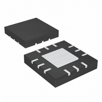
MAX9725AETC+T Maxim Integrated Products, MAX9725AETC+T Datasheet - Page 10

MAX9725AETC+T
Manufacturer Part Number
MAX9725AETC+T
Description
IC AMP AUDIO .025W STER 12TQFN
Manufacturer
Maxim Integrated Products
Series
DirectDrive™r
Type
Class ABr
Datasheet
1.MAX9725CETCT.pdf
(17 pages)
Specifications of MAX9725AETC+T
Output Type
Headphones, 2-Channel (Stereo)
Max Output Power X Channels @ Load
25mW x 2 @ 16 Ohm
Voltage - Supply
900 mV ~ 1.8 V
Features
Depop, Short-Circuit Protection, Shutdown
Mounting Type
Surface Mount
Package / Case
12-TQFN Exposed Pad
Lead Free Status / RoHS Status
Lead free / RoHS Compliant
1V, Low-Power, DirectDrive, Stereo Headphone
Amplifier with Shutdown
Figure 4. Output Power vs. Supply Voltage with Inputs In-/Out-
of-Phase
In conventional single-supply audio drivers, the output-
coupling capacitor is a major contributor of audible
clicks and pops. Upon startup, the driver charges the
coupling capacitor to its bias voltage, typically half the
supply. Likewise, on shutdown, the capacitor is dis-
charged to GND. This results in a DC shift across the
capacitor that appears as an audible transient at the
speaker. The MAX9725’s DirectDrive technology elimi-
nates the need for output-coupling capacitors.
The MAX9725 also features extensive click-and-pop
suppression that eliminates any audible transient
sources internal to the device. The Power-Up/-Down
Waveform in the Typical Operating Characteristics
shows minimal DC shift and no spurious transients at
the output upon startup or shutdown.
In most applications, the output of the preamplifier dri-
ving the MAX9725 has a DC bias of typically half the
supply. At startup, the input-coupling capacitor is
charged to the preamplifier’s DC bias voltage through
the internal input resistor (25kΩ for MAX9725A-
MAX9725D, minimum 10kΩ for MAX9725E) causing an
audible click and pop. Delaying the rise of SHDN 4 or 5
time constants, based on R
up of the preamplifier eliminates any click and pop
caused by the input filter (see the Functional Diagrams ).
10
______________________________________________________________________________________
50
45
40
35
30
25
20
15
10
5
0
0.9
OUTPUT POWER vs. SUPPLY VOLTAGE
WITH INPUTS IN- AND OUT-OF-PHASE
f
R
THD+N = 1%
IN
L
= 1kHz
= 16Ω
Click-and-Pop Suppression
SUPPLY VOLTAGE (V)
INPUTS 180 ° OUT-OF-PHASE
1.1
INPUTS IN-PHASE
IN
x C
1.3
IN
, relative to the start-
1.5
Linear power amplifiers can dissipate a significant
amount of power under normal operating conditions.
The maximum power dissipation for each package is
given in the Absolute Maximum Ratings section under
Continuous Power Dissipation or can be calculated by
the following equation:
where T
ture, and θ
°C/W as specified in the Absolute Maximum Ratings
section. For example, θ
+59.3°C/W.
The MAX9725 has two power dissipation sources, the
charge pump and the two amplifiers. If the power dissi-
pation exceeds the rated package dissipation, reduce
V
temperature, or add heatsinking to the device. Large
output, supply, and ground traces decrease θ
ing more heat to be transferred from the package to
surrounding air.
The MAX9725’s output power increases when the left
and right audio signals differ in magnitude and/or
phase. Figure 4 shows the two extreme cases for in-
and out-of-phase input signals. The output power of a
typical stereo application lies between the two extremes
shown in Figure 4. The MAX9725 is specified to output
20mW per channel when both inputs are in-phase.
The MAX9725 internally generates a negative supply
voltage (PV
signal. Other devices can be powered from PV
vided the current drawn from the charge pump does
not exceed 1mA. Headphone driver output power and
THD+N will be adversely affected if more than 1mA is
drawn from PV
cal application for the negative supply.
PV
a 1µF capacitor from C1P to C1N for best charge-pump
operation.
DD
SS
, increase load impedance, decrease the ambient
is unregulated and proportional to V
J(MAX)
P
DISSPKG(MAX)
JA
SS
) to provide the ground-referenced output
is the reciprocal of the derating factor in
SS
is +150°C, T
Applications Information
. Using PV
Powering Other Circuits from
JA
=
for the thin QFN package is
SS
T
A
the Negative Supply
J(MAX)
as an LCD bias is a typi-
is the ambient tempera-
Power Dissipation
θ
JA
- T
A
Output Power
DD
. Connect
JA
SS
, allow-
pro-


