NCP2890AFCT2G ON Semiconductor, NCP2890AFCT2G Datasheet - Page 6
NCP2890AFCT2G
Manufacturer Part Number
NCP2890AFCT2G
Description
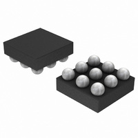
IC AMP AUDIO POWER 1W 9-FLIPCHIP
Manufacturer
ON Semiconductor
Type
Class ABr
Datasheet
1.NCP2890AFCT2G.pdf
(16 pages)
Specifications of NCP2890AFCT2G
Output Type
1-Channel (Mono)
Max Output Power X Channels @ Load
1.08W x 1 @ 8 Ohm
Voltage - Supply
2.2 V ~ 5.5 V
Features
Depop, Differential Inputs, Short-Circuit and Thermal Protection, Shutdown
Mounting Type
Surface Mount
Package / Case
9-FlipChip
Operational Class
Class-AB
Audio Amplifier Output Configuration
1-Channel Mono
Output Power (typ)
1.08x1@8OhmW
Audio Amplifier Function
Speaker
Total Harmonic Distortion
0.04%%
Single Supply Voltage (typ)
3/5V
Dual Supply Voltage (typ)
Not RequiredV
Power Supply Requirement
Single
Power Dissipation
650mW
Rail/rail I/o Type
No
Power Supply Rejection Ratio
75dB
Single Supply Voltage (min)
2.2V
Single Supply Voltage (max)
5.5V
Dual Supply Voltage (min)
Not RequiredV
Dual Supply Voltage (max)
Not RequiredV
Operating Temp Range
-40C to 85C
Operating Temperature Classification
Industrial
Mounting
Surface Mount
Pin Count
9
Package Type
Flip-Chip
Lead Free Status / RoHS Status
Lead free / RoHS Compliant
Other names
NCP2890AFCT2G
NCP2890AFCT2GOSTR
NCP2890AFCT2GOSTR
Available stocks
Company
Part Number
Manufacturer
Quantity
Price
Company:

Part Number:
NCP2890AFCT2G
Manufacturer:
ON Semiconductor
Quantity:
1 300
Part Number:
NCP2890AFCT2G
Manufacturer:
ON/安森美
Quantity:
20 000


0.001
0.001
0.01
0.01
1700
1500
1300
1100
0.1
0.1
900
700
500
300
100
10
10
1
1
0
0
2.0
Figure 11. Output Power versus Power Supply
f = 1 kHz
R
Figure 7. THD + N versus Power Out
Figure 9. THD + N versus Power Out
V
R
1 kHz
A
L
100
V
p
L
= 8 W
2.5
V
R
1 kHz
A
= 3.3 V
= 8 W
= 2
V
p
L
= 2.6 V
= 8 W
= 2
100
P
P
200
out
out
3.0
POWER SUPPLY (V)
, POWER OUT (mW)
, POWER OUT (mW)
300
200
3.5
TYPICAL PERFORMANCE CHARACTERISTICS
THD+N = 10%
400
4.0
300
THD+N = 1%
500
NCP2890, NCV2890
4.5
http://onsemi.com
600
400
5.0
6
0.001
0.01
0.01
−30
−35
−40
−45
−50
−55
−60
−65
−70
0.1
0.1
10
10
1
1
0
0
10
V
R
R
A
V
C
V
ripple
p
L
in
bypass
Figure 10. THD + N versus Power Out
= 5 V
= 8 W
= 2
Figure 8. THD + N versus Power Out
= 10 W
V
R
1 kHz
A
V
R
1 kHz
A
100
100
= 200 mV
V
p
L
V
p
L
= 1 mF
= 2.6 V
= 2
= 4 W
Figure 12. P
= 3 V
= 8 W
= 2
100
P
P
out
out
pk−pk
FREQUENCY (Hz)
, POWER OUT (mW)
, POWER OUT (mW)
200
200
1000
SRR
@ V
300
300
p
= 5 V
10,000
400
400
100,000
500
500
Related parts for NCP2890AFCT2G
Image
Part Number
Description
Manufacturer
Datasheet
Request
R

Part Number:
Description:
1w Audio Power Amplifier
Manufacturer:
ON Semiconductor
Datasheet:

Part Number:
Description:
EVAL BOARD FOR NCP2890
Manufacturer:
ON Semiconductor
Datasheet:
Part Number:
Description:
ON Semiconductor [VOLTAGE REGULATOR]
Manufacturer:
ON Semiconductor
Datasheet:
Part Number:
Description:
357-036-542-201 CARDEDGE 36POS DL .156 BLK LOPRO
Manufacturer:
ON Semiconductor
Datasheet:
Part Number:
Description:
357-036-542-201 CARDEDGE 36POS DL .156 BLK LOPRO
Manufacturer:
ON Semiconductor
Datasheet:
Part Number:
Description:
357-036-542-201 CARDEDGE 36POS DL .156 BLK LOPRO
Manufacturer:
ON Semiconductor
Datasheet:
Part Number:
Description:
357-036-542-201 CARDEDGE 36POS DL .156 BLK LOPRO
Manufacturer:
ON Semiconductor
Datasheet:
Part Number:
Description:
357-036-542-201 CARDEDGE 36POS DL .156 BLK LOPRO
Manufacturer:
ON Semiconductor
Datasheet:
Part Number:
Description:
357-036-542-201 CARDEDGE 36POS DL .156 BLK LOPRO
Manufacturer:
ON Semiconductor
Datasheet:
Part Number:
Description:
357-036-542-201 CARDEDGE 36POS DL .156 BLK LOPRO
Manufacturer:
ON Semiconductor
Datasheet:
Part Number:
Description:
357-036-542-201 CARDEDGE 36POS DL .156 BLK LOPRO
Manufacturer:
ON Semiconductor
Datasheet:
Part Number:
Description:
357-036-542-201 CARDEDGE 36POS DL .156 BLK LOPRO
Manufacturer:
ON Semiconductor
Datasheet:
Part Number:
Description:
357-036-542-201 CARDEDGE 36POS DL .156 BLK LOPRO
Manufacturer:
ON Semiconductor
Datasheet:
Part Number:
Description:
Manufacturer:
ON Semiconductor
Datasheet: