NCP2890AFCT2G ON Semiconductor, NCP2890AFCT2G Datasheet - Page 4
NCP2890AFCT2G
Manufacturer Part Number
NCP2890AFCT2G
Description
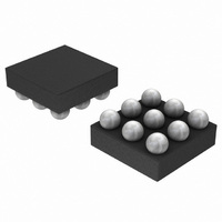
IC AMP AUDIO POWER 1W 9-FLIPCHIP
Manufacturer
ON Semiconductor
Type
Class ABr
Datasheet
1.NCP2890AFCT2G.pdf
(16 pages)
Specifications of NCP2890AFCT2G
Output Type
1-Channel (Mono)
Max Output Power X Channels @ Load
1.08W x 1 @ 8 Ohm
Voltage - Supply
2.2 V ~ 5.5 V
Features
Depop, Differential Inputs, Short-Circuit and Thermal Protection, Shutdown
Mounting Type
Surface Mount
Package / Case
9-FlipChip
Operational Class
Class-AB
Audio Amplifier Output Configuration
1-Channel Mono
Output Power (typ)
1.08x1@8OhmW
Audio Amplifier Function
Speaker
Total Harmonic Distortion
0.04%%
Single Supply Voltage (typ)
3/5V
Dual Supply Voltage (typ)
Not RequiredV
Power Supply Requirement
Single
Power Dissipation
650mW
Rail/rail I/o Type
No
Power Supply Rejection Ratio
75dB
Single Supply Voltage (min)
2.2V
Single Supply Voltage (max)
5.5V
Dual Supply Voltage (min)
Not RequiredV
Dual Supply Voltage (max)
Not RequiredV
Operating Temp Range
-40C to 85C
Operating Temperature Classification
Industrial
Mounting
Surface Mount
Pin Count
9
Package Type
Flip-Chip
Lead Free Status / RoHS Status
Lead free / RoHS Compliant
Other names
NCP2890AFCT2G
NCP2890AFCT2GOSTR
NCP2890AFCT2GOSTR
Available stocks
Company
Part Number
Manufacturer
Quantity
Price
Company:

Part Number:
NCP2890AFCT2G
Manufacturer:
ON Semiconductor
Quantity:
1 300
Part Number:
NCP2890AFCT2G
Manufacturer:
ON/安森美
Quantity:
20 000


ELECTRICAL CHARACTERISTICS
6. Min/Max limits are guaranteed by design, test or statistical analysis.
7. This parameter is not tested in production for 9−Pin Flip−Chip CSP package in case of a 5.0 V power supply.
8. See page 11 for a theoretical approach of this parameter.
9. For this parameter, the Min/Max values are given for information.
Supply Quiescent Current
Common Mode Voltage
Shutdown Current
Shutdown Voltage High
Shutdown Voltage Low
Turning On Time (Note 8)
Output Swing
Rms Output Power
Maximum Power Dissipation (Note 8)
Output Offset Voltage
Signal−to−Noise Ratio
Positive Supply Rejection Ratio
Efficiency
Thermal Shutdown Temperature (Note 9)
Total Harmonic Distortion
Characteristic
Limits apply for T
PSRR V+
V
Symbol
P
loadpeak
V
V
SNR
THD
T
V
V
Dmax
I
T
I
SDIH
SDIL
P
SD
WU
dd
h
cm
OS
sd
O
NCP2890, NCV2890
http://onsemi.com
A
between −40°C to +85°C (Unless otherwise noted).
V
p
V
Input Terminated with 10 W
V
= 5.0 V, R
p
V
p
V
V
V
V
V
= 2.6 V, P
V
Vp
R
R
p
G = 2.0, R
V
V
= 5.0 V, P
p
p
p
p
p
10 Hz < F < 20 kHz
10 Hz < F < 20 kHz
V
p
4
V
L
= 5.0 V, F = 1.0 kHz
L
p
p
THD + N < 0.1%
THD + N < 0.1%
THD + N < 0.1%
= 2.6 V, R
= 2.6 V, R
= 2.6 V, R
= 5.0 V, R
= 5.0 V, R
p
p
ripple_pp
= 2.6, F = 1.0 kHz
V
V
= 4.0 W, A
= 8.0 W, A
= 2.6 V, No Load
= 5.0 V, No Load
C
P
= 2.6 V, G = 2.0
p
p
= 5.0 V, G = 10
Conditions
F = 1.0 kHz
P
F = 217 Hz
C
V
V
V
V
V
V
V
V
O
by
= 2.6 V, 8 W
= 5.0 V, 8 W
O
by
p
p
p
p
p
p
p
p
= 0.32 W
L
= 2.6 V
= 5.0 V
= 1.0 mF
= 5.0 V
= 3.0 V
= 2.6 V
= 5.0 V
= 3.0 V
= 2.6 V
= 1.0 W
= 1 mF
−
−
−
−
orms
= 8.0 W (Note 7)
orms
= 200 mV
L
L
L
L
L
L
= 8.0 W
V
V
= 8.0 W
= 4.0 W
= 8.0 W
= 8.0 W
= 8.0 W
= 320 mW
= 1.0 W
= 2.0
= 2.0
(Note 6)
Min
−30
140
1.2
2.0
4.0
−
−
−
−
−
−
−
−
−
−
−
−
−
−
−
−
−
−
−
−
−
−
−
−
−
−
−
V
2.12
4.15
0.36
0.28
1.08
0.04
0.02
Typ
285
−64
−72
−73
−64
−74
−75
160
1.5
1.7
1.7
1.9
10
84
77
48
63
p
−
−
−
−
−
−
−
/2
(Note 6)
Max
0.65
600
180
5.5
0.4
30
4
−
−
−
−
−
−
−
−
−
−
−
−
−
−
−
−
−
−
−
−
−
−
−
Unit
mA
mV
ms
nA
dB
dB
°C
W
W
%
%
V
V
V
V
Related parts for NCP2890AFCT2G
Image
Part Number
Description
Manufacturer
Datasheet
Request
R

Part Number:
Description:
1w Audio Power Amplifier
Manufacturer:
ON Semiconductor
Datasheet:

Part Number:
Description:
EVAL BOARD FOR NCP2890
Manufacturer:
ON Semiconductor
Datasheet:
Part Number:
Description:
ON Semiconductor [VOLTAGE REGULATOR]
Manufacturer:
ON Semiconductor
Datasheet:
Part Number:
Description:
357-036-542-201 CARDEDGE 36POS DL .156 BLK LOPRO
Manufacturer:
ON Semiconductor
Datasheet:
Part Number:
Description:
357-036-542-201 CARDEDGE 36POS DL .156 BLK LOPRO
Manufacturer:
ON Semiconductor
Datasheet:
Part Number:
Description:
357-036-542-201 CARDEDGE 36POS DL .156 BLK LOPRO
Manufacturer:
ON Semiconductor
Datasheet:
Part Number:
Description:
357-036-542-201 CARDEDGE 36POS DL .156 BLK LOPRO
Manufacturer:
ON Semiconductor
Datasheet:
Part Number:
Description:
357-036-542-201 CARDEDGE 36POS DL .156 BLK LOPRO
Manufacturer:
ON Semiconductor
Datasheet:
Part Number:
Description:
357-036-542-201 CARDEDGE 36POS DL .156 BLK LOPRO
Manufacturer:
ON Semiconductor
Datasheet:
Part Number:
Description:
357-036-542-201 CARDEDGE 36POS DL .156 BLK LOPRO
Manufacturer:
ON Semiconductor
Datasheet:
Part Number:
Description:
357-036-542-201 CARDEDGE 36POS DL .156 BLK LOPRO
Manufacturer:
ON Semiconductor
Datasheet:
Part Number:
Description:
357-036-542-201 CARDEDGE 36POS DL .156 BLK LOPRO
Manufacturer:
ON Semiconductor
Datasheet:
Part Number:
Description:
357-036-542-201 CARDEDGE 36POS DL .156 BLK LOPRO
Manufacturer:
ON Semiconductor
Datasheet:
Part Number:
Description:
Manufacturer:
ON Semiconductor
Datasheet: