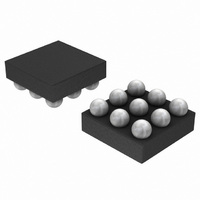
NCP2991FCT2G ON Semiconductor, NCP2991FCT2G Datasheet - Page 3

NCP2991FCT2G
Manufacturer Part Number
NCP2991FCT2G
Description
IC PWR AMP AUDIO 1.35W 9-CSP
Manufacturer
ON Semiconductor
Type
Class ABr
Datasheet
1.NCP2991FCT2G.pdf
(15 pages)
Specifications of NCP2991FCT2G
Output Type
1-Channel (Mono)
Max Output Power X Channels @ Load
1.35W x 1 @ 8 Ohm
Voltage - Supply
2.5 V ~ 5.5 V
Features
Depop, Shutdown, Thermal Protection
Mounting Type
Surface Mount
Package / Case
9-FlipChip
Operational Class
Class-AB
Audio Amplifier Output Configuration
1-Channel Mono
Audio Amplifier Function
Speaker
Single Supply Voltage (typ)
3/5V
Dual Supply Voltage (typ)
Not RequiredV
Power Supply Requirement
Single
Power Dissipation
650mW
Rail/rail I/o Type
No
Single Supply Voltage (min)
2.5V
Single Supply Voltage (max)
5.5V
Dual Supply Voltage (min)
Not RequiredV
Dual Supply Voltage (max)
Not RequiredV
Operating Temp Range
-40C to 85C
Operating Temperature Classification
Industrial
Mounting
Surface Mount
Pin Count
9
Lead Free Status / RoHS Status
Lead free / RoHS Compliant
Available stocks
Company
Part Number
Manufacturer
Quantity
Price
Part Number:
NCP2991FCT2G
Manufacturer:
ON/安森美
Quantity:
20 000
Stresses exceeding Maximum Ratings may damage the device. Maximum Ratings are stress ratings only. Functional operation above the
Recommended Operating Conditions is not implied. Extended exposure to stresses above the Recommended Operating Conditions may affect
device reliability.
1. Maximum electrical ratings are defined as those values beyond which damage to the device may occur at T
2. The thermal shutdown set to 160°C (typical) avoids irreversible damage on the device due to power dissipation.
3. The R
4. Human Body Model, 100 pF discharge through a 1.5 kW resistor following specification JESD22/A114.
5. Machine Model, 200 pF discharged through all pins following specification JESD22/A115.
PIN DESCRIPTION
MAXIMUM RATINGS
Supply Voltage
Operating Supply Voltage
Input Voltage
Power Dissipation (Note 2)
Operating Ambient Temperature
Max Junction Temperature
Storage Temperature Range
Thermal Resistance Junction−to−Air
ESD Protection
Latchup Current @ T
500 mm
Pin
A1
A2
A3
B1
B2
B3
C1
C2
C3
qJA
2
. The bumps have the same thermal resistance and all need to be connected to optimize the power dissipation.
is highly dependent of the PCB Heatsink area. For example, R
SHUTDOWN
BYPASS
OUTA
OUTB
Name
TON
INM
INP
VM
VP
A
= 85°C (Note 6)
(Note 1)
Type
O
O
I
I
I
I
I
I
I
Rating
Human Body Model (HBM) (Note 4)
Negative input of the first amplifier, receives the audio input signal. Connected to the feedback
resistor R
Negative output of the NCP2991. Connected to the load and to the feedback resistor Rf.
Positive input of the first amplifier, receives the common mode voltage.
Analog Ground.
TON pin selects 2 different Turn On times:
TON = GND −> 30 ms
TON = VP −> 15 ms
Positive analog supply of the cell. Range: 2.5 V−5.5 V.
Bypass capacitor pin which provides the common mode voltage (Vp/2).
Positive output of the NCP2991. Connected to the load.
The device enters in shutdown mode when a low level is applied on this pin.
Machine Model (MM) (Note 5)
f
and to the input resistor R
http://onsemi.com
3
qJA
can equal 195°C/W with 50 mm
in
.
Description
Symbol
Op Vp
R
T
V
Pd
V
T
T
stg
qJA
−
−
A
in
J
p
Internally Limited
−0.3 to V
−65 to +150
2
2.5 to 5.5 V
−40 to +85
(Note 3)
total area and also 135°C/W with
A
Value
2000
±100
150
200
= +25°C.
6.0
CC
+0.3
°C/W
Unit
mA
°C
°C
°C
V
V
V
−
−


