NCP2991FCT2G ON Semiconductor, NCP2991FCT2G Datasheet
NCP2991FCT2G
Specifications of NCP2991FCT2G
Available stocks


Related parts for NCP2991FCT2G

NCP2991FCT2G Summary of contents
Page 1
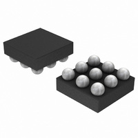
... PDAs • Wireless Phones *For additional information on our Pb−Free strategy and soldering details, please download the ON Semiconductor Soldering and Mounting Techniques Reference Manual, SOLDERRM/D. © Semiconductor Components Industries, LLC, 2009 November, 2009 − Rev. 2 http://onsemi.com 9−Pin Flip−Chip CSP ...
Page 2
Ci Ri INM AUDIO INPUT INP 100 BYPASS bypass SHUTDOWN Connect to V Figure 1. Typical Audio Amplifier Application Circuit with Single Ended Input 100 INM AUDIO INP ...
Page 3
PIN DESCRIPTION Pin Name Type A1 INM I Negative input of the first amplifier, receives the audio input signal. Connected to the feedback resistor R A2 OUTA O Negative output of the NCP2991. Connected to the load and to the ...
Page 4
ELECTRICAL CHARACTERISTICS Limits apply for T Characteristic Supply Quiescent Current Common Mode Voltage Shutdown Current Shutdown Pull−Down Shutdown Voltage High Shutdown Voltage Low Turn On Time (Note 8) Turn Off Time Output Impedance in Shutdown Mode Output Swing RMS Output ...
Page 5
FREQUENCY (Hz) Figure 3. THD+N vs. Frequency 1 0.1 0.01 100 1,000 FREQUENCY (Hz) Figure 5. THD+N vs. Frequency 1 0.1 0.01 100 1,000 FREQUENCY (Hz) Figure 7. THD+N vs. Frequency TYPICAL CHARACTERISTICS 1 THD+N ...
Page 6
THD 2 out R L 0.1 Differential Input 0.01 0.001 100 1,000 FREQUENCY (Hz) Figure 9. THD+N vs. Frequency 1 0.1 0.01 100 1,000 FREQUENCY (Hz) Figure 11. THD+N vs. Frequency 1 0.1 0.01 100 ...
Page 7
0.1 0.01 0 400 100 3.3 V 0.1 0.01 0.001 0 500 −50 −60 −70 −80 −90 −100 −110 10 100 1000 FREQUENCY (Hz) Figure 17. ...
Page 8
FREQUENCY (Hz) Figure 19. PSRR vs. Frequency −50 −60 −70 −80 −90 −100 −110 10 100 1000 FREQUENCY (Hz) Figure 21. PSRR vs. Frequency 800 700 600 500 400 300 ...
Page 9
Ch1 : OUTA Ch2 : OUTB Ch3 : / Ch1 – Ch2 : Differential signal seen by the load Figure 25. Zero pop noise turn on sequence with ...
Page 10
Ch1 : OUTA Ch2 : OUTB Ch3 : / Ch1 – Ch2 : Differential signal seen by the load Figure 29. Zero pop noise turn on sequence with differential input to ground (Ci = 100 nF ...
Page 11
Ch1 : OUTA Ch2 : OUTB Ch3 : / Ch1 – Ch2 : Differential signal seen by the load Figure 33. Zero pop noise turn on sequence with single-ended input to ground ( nF ...
Page 12
Ch1 : OUTA Ch2 : OUTB Ch3 : / Ch1 – Ch2 : Differential signal seen by the load Figure 37. Zero pop noise turn on sequence with differential input to ground ( nF ...
Page 13
Detailed Description The NCP2991 audio amplifier can operate under 2.5 V until 5.5 V power supply. With less than 1% THD + N, it can deliver up to 1.35 W RMS output power to an 8.0 W load (V = ...
Page 14
... Depending on the test, user can consider different level of protection: ORDERING INFORMATION Device NCP2991FCT2G †For information on tape and reel specifications, including part orientation and tape sizes, please refer to our Tape and Reel Packaging Specifications Brochure, BRD8011/D. − capacitor connected between each amplifier output terminals and ground. − ...
Page 15
... SCILLC is an Equal Opportunity/Affirmative Action Employer. This literature is subject to all applicable copyright laws and is not for resale in any manner. PUBLICATION ORDERING INFORMATION LITERATURE FULFILLMENT: Literature Distribution Center for ON Semiconductor P.O. Box 5163, Denver, Colorado 80217 USA Phone: 303−675−2175 or 800−344−3860 Toll Free USA/Canada Fax: 303− ...