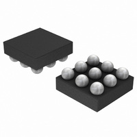
NCP2991FCT2G ON Semiconductor, NCP2991FCT2G Datasheet - Page 11

NCP2991FCT2G
Manufacturer Part Number
NCP2991FCT2G
Description
IC PWR AMP AUDIO 1.35W 9-CSP
Manufacturer
ON Semiconductor
Type
Class ABr
Datasheet
1.NCP2991FCT2G.pdf
(15 pages)
Specifications of NCP2991FCT2G
Output Type
1-Channel (Mono)
Max Output Power X Channels @ Load
1.35W x 1 @ 8 Ohm
Voltage - Supply
2.5 V ~ 5.5 V
Features
Depop, Shutdown, Thermal Protection
Mounting Type
Surface Mount
Package / Case
9-FlipChip
Operational Class
Class-AB
Audio Amplifier Output Configuration
1-Channel Mono
Audio Amplifier Function
Speaker
Single Supply Voltage (typ)
3/5V
Dual Supply Voltage (typ)
Not RequiredV
Power Supply Requirement
Single
Power Dissipation
650mW
Rail/rail I/o Type
No
Single Supply Voltage (min)
2.5V
Single Supply Voltage (max)
5.5V
Dual Supply Voltage (min)
Not RequiredV
Dual Supply Voltage (max)
Not RequiredV
Operating Temp Range
-40C to 85C
Operating Temperature Classification
Industrial
Mounting
Surface Mount
Pin Count
9
Lead Free Status / RoHS Status
Lead free / RoHS Compliant
Available stocks
Company
Part Number
Manufacturer
Quantity
Price
Part Number:
NCP2991FCT2G
Manufacturer:
ON/安森美
Quantity:
20 000
single-ended input to ground (Ci = 47 nF, Ri = 24 kW,
single-ended input to ground (Ci = 47 nF, Ri = 24 kW,
Figure 33. Zero pop noise turn on sequence with
Figure 35. Zero pop noise turn off sequence with
Rf = 24 kW, Cbyp = 1 mF, Rl = 8 W, Ton = Vp)
Rf = 24 kW, Cbyp = 1 mF, Rl = 8 W, Ton = Vp)
Ch1 : OUTA
Ch2 : OUTB
Ch3 : /SD
M1 = Ch1 – Ch2 : Differential
signal seen by the load
Ch1 : OUTA
Ch2 : OUTB
Ch3 : /SD
M1 = Ch1 – Ch2 : Differential
signal seen by the load
http://onsemi.com
11
24 kW, Rf = 24 kW, Cbyp = 1 mF, Rl = 8 W, Ton = Vp)
24 kW, Rf = 24 kW, Cbyp = 1 mF, Rl = 8 W, Ton = Vp)
Figure 34. Zero pop noise turn on sequence with
single-ended input audio source (Ci = 47 nF, Ri =
Figure 36. Zero pop noise turn off sequence with
single-ended input audio source (Ci = 47 nF, Ri =
Ch1 : OUTA
Ch2 : OUTB
Ch3 : /SD
M1 = Ch1 – Ch2 : Differential
signal seen by the load
Ch1 : OUTA
Ch2 : OUTB
Ch3 : /SD
M1 = Ch1 – Ch2 : Differential
signal seen by the load


