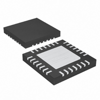
MAX9850ETI+ Maxim Integrated Products, MAX9850ETI+ Datasheet - Page 27

MAX9850ETI+
Manufacturer Part Number
MAX9850ETI+
Description
IC AMP AUDIO .095W STER 28TQFN
Manufacturer
Maxim Integrated Products
Series
DirectDrive™r
Type
Class ABr
Datasheet
1.MAX9850ETI.pdf
(36 pages)
Specifications of MAX9850ETI+
Output Type
Headphones, 2-Channel (Stereo)
Max Output Power X Channels @ Load
95mW x 2 @ 16 Ohm
Voltage - Supply
1.8 V ~ 3.6 V
Features
DAC, Depop, Digital Inputs, I²C, I²S, Line Level Inputs & Outputs, Mute, Shutdown, Volume Control
Mounting Type
Surface Mount
Package / Case
28-WQFN Exposed Pad, 28-HWQFN
Product
General Purpose Audio Amplifiers
Output Power
95 mW
Operating Supply Voltage
1.8 V to 3.6 V
Supply Current
7.6 mA
Maximum Power Dissipation
2857 mW
Maximum Operating Temperature
+ 85 C
Mounting Style
SMD/SMT
Minimum Operating Temperature
- 40 C
Supply Voltage (max)
3.6 V
Supply Voltage (min)
1.8 V
Lead Free Status / RoHS Status
Lead free / RoHS Compliant
00 = Headphone volume slews from code 0x00 to 0x28
in 63µs. Not recommended when ZDEN = 1.
01 = Headphone volume slews from code 0x00 to 0x28
in 125ms.
10 = Headphone volume slews from code 0x00 to 0x28
in 63ms.
11 = Headphone volume slews from code 0x00 to 0x28
in 42ms.
Program SR(1:0) to set the rate that the MAX9850 uses to
slew between two volume settings. The slew-rate control
also controls the amount of time the headphone outputs
take to mute or shut down after the command is given.
CP(4:0) controls the charge-pump clock divider. The
charge-pump clock frequency (f
either ICLK or from the internal oscillator.
Program CP(4:0) = 0x00 to enable the 667kHz internal
oscillator. This allows the headphone amplifiers and
line outputs to operate when the DAC is disabled.
Programming CP(4:0) to any value other than 0x00 dis-
ables the internal oscillator and derives the charge-
pump clock from ICLK. Program CP(4:0) with a value
that creates a 667kHz ±20% charge-pump clock from
ICLK by the following equation:
where:
f
N
greater than 1 when deriving the charge-pump clock
from I
f
667kHz ±20% for proper operation.
SF = MCLK scale factor. SF is the decimal value of
IC(1:0) + 1.
Table 19. LRCLK MSB (0x8) and LRCLK
LSB (0x9) Read/Write, Bit Descriptions
MCLK
CP
CP(4:0)
INT
B7
= charge-pump clock frequency. Program f
CLK
LRCLK MSB and LRCLK LSB Registers
= MCLK frequency.
= decimal value of CP(4:0). N
B6
.
f
CP
Charge-Pump Clock Divider (CP(4:0))
B5
=
______________________________________________________________________________________
2
×
B4
NCP
LSB(7:0)
f
MCLK
Slew-Rate Control (SR(1:0))
MSB(14:8)
( : )
4 0
B3
Stereo Audio DAC with DirectDrive
×
CPCLK
SF
B2
) is derived from
CP(4:0)
B1
must be
CP
B0
=
1 = Configure the MAX9850 to integer mode.
0 = Configure the MAX9850 to noninteger mode.
Integer mode operation requires that ICLK is an integer
multiple of 16 times the sample rate (f
DAC Operating Modes section. When in integer mode,
f
MSB(14:8) and LSB(7:0) are used to determine f
when in noninteger mode only (see the DAC Operating
Modes section). For noninteger mode:
LSB(7:0) combined with MSB(14:8) sets the LRCLK
divider when the MAX9850 is configured in noninteger
mode. Only LSB(7:0) is used to determine f
the MAX9850 is configured in integer mode. See the
DAC Operating Modes section.
1 = Configure the MAX9850 to master mode.
0 = Configure the MAX9850 to slave mode.
Set MAS = 1 to configure the MAX9850 to master mode.
The LRCLK and BCLK are generated by the MAX9850
when in master mode. Set MAS = 0 to configure the
MAX9850 as a digital audio slave that accepts LRCLK
and BCLK from an external digital audio source.
1 = Left audio data is clocked in when LRCLK is high
and right data is clocked in when LRCLK is low.
0 = Left audio data is clocked in when LRCLK is low
and right data is clocked in when LRCLK is high.
Set INV = 0 to conform to the I
1 = Digital data at SDIN latches in on the falling edge of
BCLK.
0 = Digital data at SDIN latches in on the rising edge of
BCLK.
Set BCINV = 0 to conform to the I
Table 20. Digital Audio (0xA) Read/Write,
Bit Descriptions
LRCLK
MAS
B7
Headphone Amplifier
= f
INV
B6
ICLK
N
BCINV
/ (16 x LSB(7:0)).
MSB LSB
B5
,
LRCLK MSB Divider (MSB(14:8))
LRCLK LSB Divider (LSB(7:0))
LSF
B4
=
2
Digital Audio Register
22
2
Bit Clock Invert (BCINV)
DLY
B3
S standard.
f
×
ICLK
2
S standard.
f
Master Mode (MAS)
LRCLK
LRCLK Invert (INV)
Integer Mode (INT)
RTJ
B2
LRCLK
LRCLK
B1
). See the
WS(1:0)
LRCLK
when
B0
27


