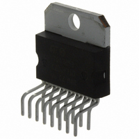
TDA7293V STMicroelectronics, TDA7293V Datasheet - Page 7

TDA7293V
Manufacturer Part Number
TDA7293V
Description
IC AMP AUDIO 100W AB MULTIWATT15
Manufacturer
STMicroelectronics
Type
Class ABr
Datasheet
1.TDA7293V.pdf
(21 pages)
Specifications of TDA7293V
Output Type
1-Channel (Mono)
Max Output Power X Channels @ Load
100W x 1 @ 4 Ohm
Voltage - Supply
±12 V ~ 50 V
Features
Depop, Differential Inputs, Mute, Short-Circuit and Thermal Protection, Standby
Mounting Type
Through Hole
Package / Case
Multiwatt-15 (Vertical, Bent and Staggered Leads)
Product
Class-AB
Output Power
100 W
Available Set Gain
80 dB
Thd Plus Noise
0.005 %
Operating Supply Voltage
+/- 60 V
Supply Current
10 A
Maximum Power Dissipation
50000 mW
Maximum Operating Temperature
+ 70 C
Mounting Style
Through Hole
Audio Load Resistance
8 Ohms
Dual Supply Voltage
+/- 15 V, +/- 18 V, +/- 24 V, +/- 28 V
Input Bias Current (max)
1 uA
Input Offset Voltage
10 mV
Input Signal Type
Single
Minimum Operating Temperature
0 C
Output Signal Type
Single
Supply Type
Dual
Amplifier Class
AB
No. Of Channels
1
Supply Voltage Range
± 12V To ± 50V
Load Impedance
4ohm
Operating Temperature Range
0°C To +70°C
Amplifier Case Style
Multiwatt15
Rohs Compliant
Yes
Lead Free Status / RoHS Status
Lead free / RoHS Compliant
Other names
497-2170-5
Available stocks
Company
Part Number
Manufacturer
Quantity
Price
Part Number:
TDA7293V
Manufacturer:
ST
Quantity:
20 000
TDA7293
3
3.1
Circuit description
In consumer electronics, an increasing demand has arisen for very high power monolithic
audio amplifiers able to match, with a low cost, the performance obtained from the best
discrete designs.
The task of realizing this linear integrated circuit in conventional bipolar technology is made
extremely difficult by the occurence of 2nd breakdown phoenomenon. It limits the safe
operating area (SOA) of the power devices, and, as a consequence, the maximum
attainable output power, especially in presence of highly reactive loads.
Moreover, full exploitation of the SOA translates into a substantial increase in circuit and
layout complexity due to the need of sophisticated protection circuits.
To overcome these substantial drawbacks, the use of power MOS devices, which are
immune from secondary breakdown is highly desirable.
The device described has therefore been developed in a mixed bipolar-MOS high voltage
technology called BCDII 100/120.
Output Stage
The main design task in developping a power operational amplifier, independently of the
technology used, is that of realization of the output stage.
The solution shown as a principle shematic by Fig6 represents the DMOS unity - gain output
buffer of the TDA7293.
Figure 4.
This large-signal, high-power buffer must be capable of handling extremely high current and
voltage levels while maintaining acceptably low harmonic distortion and good behaviour
over frequency response; moreover, an accurate control of quiescent current is required.
A local linearizing feedback, provided by differential amplifier A, is used to fullfil the above
requirements, allowing a simple and effective quiescent current setting. Proper biasing of
the power output transistors alone is however not enough to guarantee the absence of
crossover distortion.
Schematic of a DMOS unity-gain buffer
Doc ID 6744 Rev 8
Circuit description
7/21


